Method for realizing infrared photoelectric detection by regulating and controlling metal/semiconductor Schottky junction through pyroelectric effect of polar semiconductor
A Schottky junction, semiconductor technology, applied in the direction of semiconductor devices, circuits, electrical components, etc., can solve the problems of unsuitability for large-scale application, complex electrode structure, complex device structure, etc., to achieve large band gap, high detection rate, Responsive effect
- Summary
- Abstract
- Description
- Claims
- Application Information
AI Technical Summary
Problems solved by technology
Method used
Image
Examples
Embodiment 1
[0040] A method for regulating a metal / semiconductor Schottky junction through the pyroelectric effect of a polar semiconductor to realize infrared photodetection, comprising the following steps:
[0041] (1) Place the unintentionally doped sapphire substrate GaN on the sputtering table of the sputtering instrument, and use the ion sputtering coating method to deposit the gold film by ion sputtering through the template method. The sputtering target is a gold target, and the vacuum degree is for 10 -1 mbar, the current is 6mA, and the sputtering time is 120s; a gold electrode with a length of 2mm and a width of 1mm is made.
[0042] (2) Place the GaN film on the gold electrode sputtered in step (1) with 60 μW / cm 2 , In a 365nm ultraviolet light atmosphere, test its initial current at -5V-5V.
[0043] (3) Under the conditions of step (2), process under different optical power 1064nm infrared light, the free electrons excited by ultraviolet light absorb infrared light and gene...
Embodiment 2
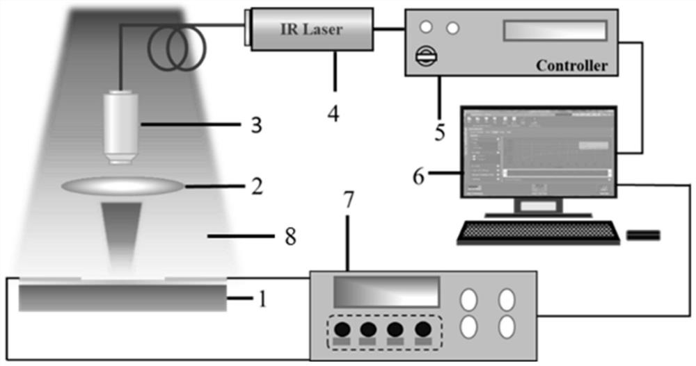
[0050] According to the method of embodiment 1, the metal / semiconductor Schottky junction is regulated and controlled through the pyroelectric effect of the polar semiconductor to realize infrared photodetection, and adopt figure 2 The experimental setup shown was tested at 60μW / cm 2 , 365nm ultraviolet light atmosphere, at 50mW / cm 2 , 1064nm infrared light switches in a period of 100s to detect the current change of the sample, the test results are as follows Figure 6 shown.
[0051] Depend on Figure 6 It can be seen that during the infrared switching process, the response speed of the sample reaches 0.5s, and the sample has good repeatability and stability.
Embodiment 3-7
[0053] Change the polar wide bandgap semiconductor material and Schottky junction material, as well as the power density of infrared light irradiation, as shown in Table 1.
[0054] Table 1
[0055] Item Number Example 3 Example 4 Example 5 Example 6 Example 7 Polar Wide Bandgap Semiconductor Materials Zinc oxide aluminum nitride Cadmium sulfide gallium oxide Silicon carbide Schottky junction material silver platinum gold silver platinum Infrared light irradiation power density mW / cm 2
PUM
| Property | Measurement | Unit |
|---|---|---|
| Power density | aaaaa | aaaaa |
Abstract
Description
Claims
Application Information
 - R&D
- Intellectual Property
- Life Sciences
- Materials
- Tech Scout
- Unparalleled Data Quality
- Higher Quality Content
- 60% Fewer Hallucinations
Browse by: Latest US Patents, China's latest patents, Technical Efficacy Thesaurus, Application Domain, Technology Topic, Popular Technical Reports.
© 2025 PatSnap. All rights reserved.Legal|Privacy policy|Modern Slavery Act Transparency Statement|Sitemap|About US| Contact US: help@patsnap.com


