Laminate, printed wiring board, semiconductor package, and method for manufacturing laminate

A laminated board and composite layer technology, which is applied in the direction of printed circuits, printed circuits, printed circuit parts, etc., can solve the problems of insulation reliability, adhesion, and reduction of pressing processability.

Active Publication Date: 2021-07-30
RESONAC CORPORATION
View PDF6 Cites 0 Cited by
  • Summary
  • Abstract
  • Description
  • Claims
  • Application Information

AI Technical Summary

Problems solved by technology

[0005] However, since the high filling of inorganic fillers has the possibility of reducing insulation reliability, adhesion with copper foil, press workability, etc., from the viewpoint of ensuring these performances, only high filling of inorganic fillers There is a limit to the high elastic modulus and low thermal expansion of the laminate due to

Method used


Image

  • Laminate, printed wiring board, semiconductor package, and method for manufacturing laminate
  • Laminate, printed wiring board, semiconductor package, and method for manufacturing laminate
  • Laminate, printed wiring board, semiconductor package, and method for manufacturing laminate

Examples


Embodiment 1

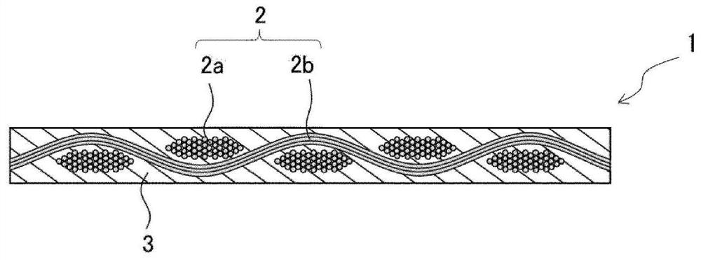
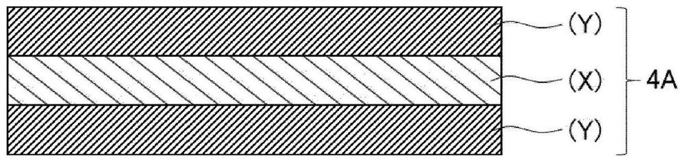
[0253] (Copper Clad Laminate 1: In Figure 6 Copper-clad laminates with copper foil disposed on both sides of the laminate shown)

[0254] (1) Production of varnish

[0255] In a reaction vessel with a capacity of 1 liter capable of heating and cooling equipped with a thermometer, a stirring device, and a reflux condenser, siloxane diamine (manufactured by Dow Corning Toray Co., Ltd., trade name: X-22-161A, an amino functional group Equivalent: 800g / mol) 19.4g, 3,3'-diethyl-4,4'-diaminodiphenylmethane 13.0g, N,N'-(4,4'-diphenylmethane) dimaline 122.9 g of imide, 4.7 g of p-aminophenol, and 240.0 g of propylene glycol monomethyl ether were reacted at 115° C., then concentrated under normal pressure so that the resin concentration became 60% by mass, and cyclohexyl was further added at 90° C. 53.3 g of the ketone was stirred for 30 minutes to obtain an intermediate varnish.

[0256] 303.5 g of this intermediate varnish, a methyl isobutyl ketone solution of silica (700 g of sp...

Embodiment 2

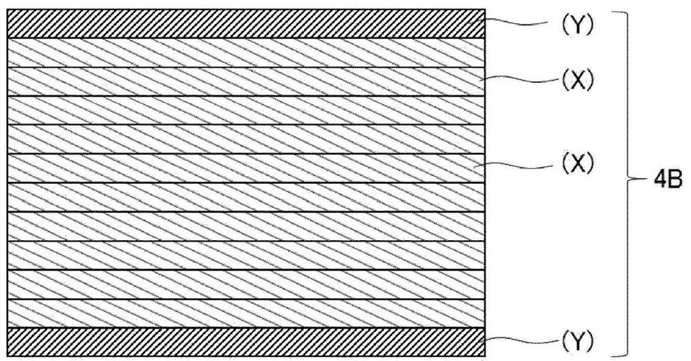
[0262] (Copper Clad Laminate 2: in Figure 4 Copper-clad laminates with copper foil disposed on both sides of the laminate shown)

[0263] In Example 1, prepregs were laminated so that the outermost layers of the two layers on both sides were prepregs containing S glass cloth, and the inner 10 layers were prepregs containing E glass cloth. , except that, it carried out similarly to Example 1, and obtained the copper-clad laminated board 2.

Embodiment 3

[0265] (Copper Clad Laminate 3: in Figure 7 Copper-clad laminates with copper foil disposed on both sides of the laminate shown)

[0266] In Example 1, the prepregs were laminated in the order of six prepregs containing E glass cloth, two prepregs containing S glass cloth, and six prepregs containing E glass cloth. Except having changed the structure, it carried out similarly to Example 1, and obtained the copper-clad laminated board 3.


PUM

PropertyMeasurementUnit
thicknessaaaaaaaaaa
particle sizeaaaaaaaaaa

Abstract

The present invention pertains to: a laminate containing two or more composite layers each containing a fiber base material and a cured product of a thermosetting resin composition, wherein the two or more composite layers contains at least one composite layer (X) and at least one composite layer (Y), the composite layer (X) contains a first fiber base material composed of a first glass fiber, the composite layer (Y) contains a second fiber base material composed of a second glass fiber, and the second glass fiber has a higher tensile modulus at 25 degrees than that of the first glass fiber; a printed wiring board using the laminate; a semiconductor package; and a method for manufacturing the laminate.

Description

technical field [0001] The present invention relates to a laminate, a printed wiring board, a semiconductor package, and a method for manufacturing the laminate. Background technique [0002] In recent years, due to miniaturization and high performance of electronic equipment, higher wiring density and higher integration of printed wiring boards have been developed. Along with this, the demand for improved reliability of printed wiring boards has been increasing. In particular, with respect to semiconductor packages, along with miniaturization and thinning, occurrence of warpage during component packaging and package assembly has become a major problem. [0003] One of the main causes of semiconductor package warpage is the difference in coefficient of thermal expansion between a semiconductor element and a printed wiring board on which the semiconductor element is mounted. Generally, since the thermal expansion coefficient of a printed wiring board is larger than that of a...

Claims


Application Information

Patent Timeline
Patent Type & Authority Applications(China)
IPC IPC(8): B32B17/04B32B17/12B32B15/20B32B15/14B32B27/04B29C70/16B29C70/30H05K1/03B29K101/10B29K105/08B29L9/00B29L7/00
CPCB29C70/30B29C70/16B32B7/022B32B5/02B32B5/024B32B5/26B32B5/263B32B2457/08B32B15/14B32B15/20B32B2250/05B32B2250/20B32B2262/101B32B2260/023B32B2260/046B32B2250/40B32B2264/104B32B2264/101B32B7/02B32B2307/732B32B2264/107B32B2307/206B32B5/022B32B2264/102H05K1/0366H05K2201/029H05K1/0271H05K2201/068B29C70/003B32B17/04H01L23/12H05K1/0306H05K1/038B29K2105/0872B32B2305/076B29K2101/10B29K2309/08B29L2009/00B32B2307/54H05K1/036
Inventor 村上德昭内村亮一尾濑昌久大桥健一
Owner RESONAC CORPORATION
Why Eureka
Try Eureka