
Ultraviolet light emitting diode, ultraviolet LED epitaxial layer structure and preparation method thereof

A technology of light-emitting diodes and epitaxial layers, which is applied to electrical components, circuits, semiconductor devices, etc., can solve the problems of high density, slow lateral closure rate of AlGaN, and inability to annihilate dislocations, so as to improve crystal quality, increase luminous intensity, and promote Effects of Diagonal Climbing

Active Publication Date: 2021-06-29
NINGBO INST OF MATERIALS TECH & ENG CHINESE ACADEMY OF SCI
View PDF7 Cites 1 Cited by
  • Summary
  • Abstract
  • Description
  • Claims
  • Application Information

AI Technical Summary

Problems solved by technology

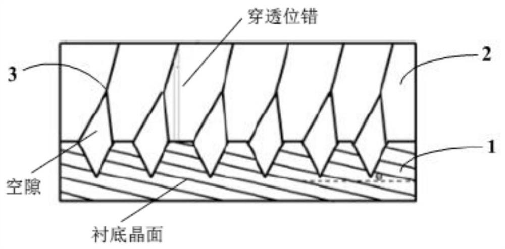
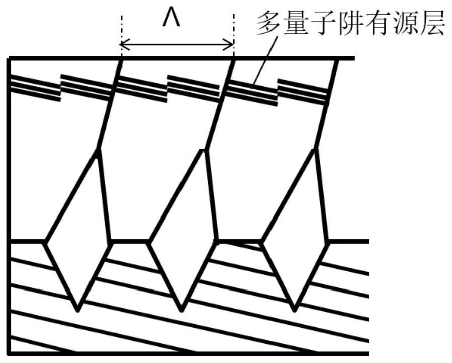
However, when growing AlN and AlGaN with high aluminum composition based on traditional PSS sapphire substrates, there are still defects that dislocations cannot be annihilated and the density is high, and the lateral closure rate of AlN and AlGaN with high aluminum composition is often slow, so that it cannot Obtain a flat, high-quality film
Moreover, since the bevel angle of the current sapphire substrate is generally 0° to 0.2°, the quantum well has a uniform and flat interface, which cannot cause the phase separation of Al and Ga in AlGaN, so that the carrier localization effect cannot be formed. , thus limiting the luminous efficiency of UV LED devices

Method used


Image

  • Ultraviolet light emitting diode, ultraviolet LED epitaxial layer structure and preparation method thereof
  • Ultraviolet light emitting diode, ultraviolet LED epitaxial layer structure and preparation method thereof
  • Ultraviolet light emitting diode, ultraviolet LED epitaxial layer structure and preparation method thereof

Examples


preparation example Construction

[0034] One aspect of the present invention provides a method for preparing an ultraviolet LED epitaxial layer structure, which includes the following steps:

[0035] Provide a nano-patterned sapphire substrate with a chamfer angle on the c-plane, the angle of the chamfer angle is 0.5°~8°;

[0036] growing an AlN epitaxial layer on the substrate;

[0037]Al growth on AlN epitaxial layer x Ga 1-x N epitaxial layer;

[0038] in Al x Ga 1-x n-Al growth on N epitaxial layer y Ga 1-y N contact layer;

[0039] in n-Al y Ga 1-y Al growth on the N contact layer m Ga 1-m N / Al n Ga 1-n N multiple quantum well active layer; and

[0040] in Al m Ga 1-m N / Al n Ga 1-n A p-type contact layer is grown on the N multi-quantum well active layer, wherein the p-type contact layer is p-Al g Ga 1-g N / p-GaN superlattice contact layer, p-Al g Ga 1-g At least one of an N contact layer and a p-GaN contact layer;

[0041] Wherein, 0.5≤x≤1, 0.5≤y≤1, 0.3≤m≤0.7, 0.3≤n≤0.7, and x≥y≥m≥n;...

Embodiment 1

[0060] Embodiment 1 Preparation of UV LED Epitaxial Layer Structure

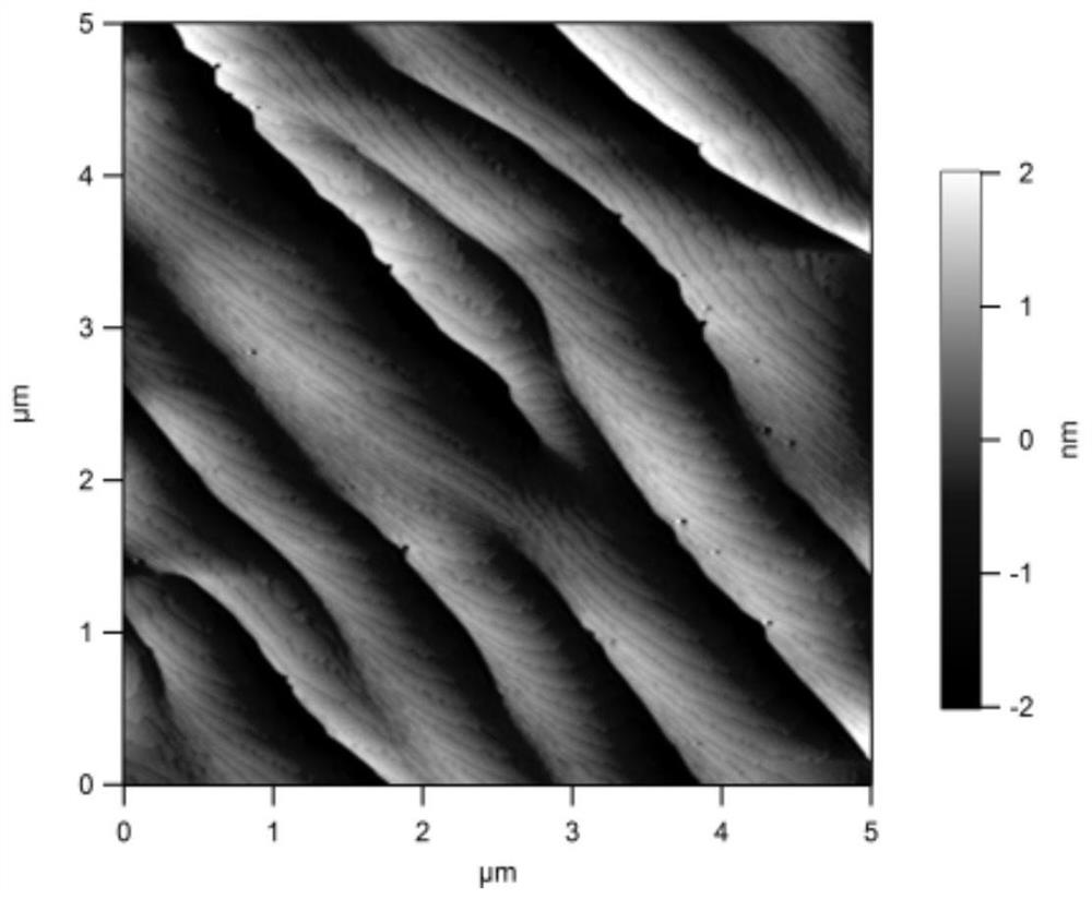
[0061] (1) Adopt a 2-inch c-plane sapphire substrate, and make a sapphire substrate in which the c-plane is inclined 0.5° toward the m-plane through a cutting process;

[0062] (2) Prepare a nano-patterned sapphire substrate with an inverted pyramid structure on the sapphire substrate in step (1) by nanoimprinting technology. The period of the nanopatterned structure on the nanopatterned sapphire substrate is 2 μm, and the depth of the inverted pyramid structure is 1 μm;

[0063] (3) Place the nanopatterned sapphire substrate in step (2) in an MOCVD device, and grow a 2 μm thick AlN epitaxial layer, an 800 nm thick Al 0.7 Ga 0.3 N epitaxial layer, 500nm thick n-Al 0.65 Ga 0.35 N and 300nm thick n-Al 0.55 Ga 0.45 The contact layer composed of N together, and further grow 80nm thick Al on the contact layer 0.6 Ga 0.4 N / Al 0.5 Ga 0.5 N multi-quantum well active layer, this layer includes 5 pairs of Al...

Embodiment 2

[0065] Embodiment 2 Preparation of UV LED Epitaxial Layer Structure

[0066] (1) Adopt a 2-inch c-plane sapphire substrate, and make a sapphire substrate in which the c-plane is inclined 2° toward the a-plane through a cutting process;

[0067] (2) Prepare a nano-patterned sapphire substrate with an inverted pyramid structure on the sapphire substrate in step (1) by nanoimprinting technology. The period of the nanopatterned structure on the nanopatterned sapphire substrate is 1 μm, and the depth of the inverted pyramid structure is 500nm;

[0068] (3) Place the nanopatterned sapphire substrate in step (2) in an MOCVD device, and grow a 2 μm thick AlN epitaxial layer, an 800 nm thick Al 0.8 Ga 0.2 N epitaxial layer, 500nm thick n-Al 0.65 Ga 0.35 N and 300nm thick n-Al 0.55 Ga 0.45 The contact layer composed of N together, and further grow 50nm thick Al on the contact layer 0.6 Ga 0.4 N / Al 0.5 Ga 0.5 N multi-quantum well active layer, this layer includes 3 pairs of Al ...


PUM

PropertyMeasurementUnit
thicknessaaaaaaaaaa
thicknessaaaaaaaaaa
thicknessaaaaaaaaaa

Abstract

The invention relates to the technical field of semiconductors, in particular to a light emitting diode, an ultraviolet LED epitaxial layer structure and a preparation method thereof. The preparation method of the ultraviolet LED epitaxial layer structure provided by the invention comprises the following steps of: providing a nano patterned sapphire substrate with a c surface having a chamfer angle of 0.5-8 degrees, whereinthe angle of the chamfer angle ranges from 0.5 to 8 degrees; and sequentially growing an AlN epitaxial layer, an AlxGa1-xN epitaxial layer, an n-AlyGa1-yN contact layer, an AlmGa1-mN / AlnGa1-nN multi-quantum well active layer and a p-type contact layer on the substrate, wherein the p-type contact layer is at least one of a p-AlgGa1-gN / p-GaN superlattice contact layer, a p-AlgGa1-gN contact layer and a p-GaN contact layer, 0.5<=x<=1, 0.5<=y<=1, 0.3<=m<=0.7, 0.3<=n<=0.7, x>=y, m>=n, and 0.5<=g<=1. According to the preparation method, effective annihilation of dislocation can be realized, the dislocation density is reduced, and formation of a carrier localization effect is promoted, so that the luminous efficiency of an ultraviolet LED device is improved. The invention further provides an ultraviolet light emitting diode chip and the ultraviolet light emitting diode.

Description

technical field [0001] The invention relates to the technical field of semiconductors, in particular to an ultraviolet light emitting diode, an ultraviolet LED epitaxial layer structure and a preparation method thereof. Background technique [0002] Compared with traditional light sources, ultraviolet light-emitting diode (ultraviolet LED) solid-state light sources based on III-V nitride materials have the advantages of high efficiency, small size, and long life. and other fields have a wide range of applications. [0003] Due to the lack of large-size, low-cost nitride single-crystal substrates, III-V nitride films are grown heteroepitaxially. Among them, sapphire (Al 2 o 3 ) has become the most widely used substrate material due to its excellent properties of large size, low price, good light transmission, good chemical stability and thermal stability. However, due to the 16% lattice mismatch between III-nitride and sapphire, a large number of dislocations and point de...

Claims


Application Information

Patent Timeline
Patent Type & Authority Applications(China)
IPC IPC(8): H01L33/06H01L33/32H01L33/04H01L33/00
CPCH01L33/06H01L33/32H01L33/04H01L33/0075Y02P70/50
Inventor 郭炜叶继春徐厚强
Owner NINGBO INST OF MATERIALS TECH & ENG CHINESE ACADEMY OF SCI
Learn More