Photoelectric chip integrated fiber manufacturing method and fiber product thereof

A technology for optoelectronic chips and integrated fibers, which is applied in the field of fiber products and optoelectronic chip integrated fibers, can solve the problems of limited fiber length, large material restrictions, and complicated preparation, so as to promote packaging and electrical connection, and solve the problem of fiber length. The effect of limited and simple craftsmanship

Inactive Publication Date: 2021-06-18
HUAZHONG UNIV OF SCI & TECH
View PDF6 Cites 0 Cited by
  • Summary
  • Abstract
  • Description
  • Claims
  • Application Information

AI Technical Summary

Problems solved by technology

Because this method can deposit different materials in sequence, it can realize a variety of in-fiber devices, such as PN junctions, Schottky junctions, PIN junctions, ohmic contacts, etc. in fibers, but this process has certain limitations. The fiber length is limited, only centimeter to millimeter-scale fibers can be realized, and it is only suitable for materials that can be synthesized in the gas phase within the fiber, which has great restrictions on the materials used
[0006] The integration of functional fiber devices by doping materials with different electrical and optical properties in fibers is complex and limited, because a variety of materials are required to realize complex functions in fibers, including crystalline semiconductor materials, high-melting point alloys, Films, thermosetting polymers, etc., and these materials are often unable to achieve co-drawing with fiber materials. Due to the limitations of these materials and the requirements of micro-scale size control for micro-electronic devices, this method is used to fully integrate micro-electronic devices into fiber is not feasible
[0007] Chinese invention patent CN208385024U discloses a fibrous electrode and a fibrous energy harvesting device, wherein the fibrous electrode uses polydimethylsiloxane as the inner core, and its surface is coated with single-walled carbon nanotubes as the inner conductive nanolayer , and lead out the copper wire from one end, then add the piezoelectric nanomaterial layer and the outer conductive nanomaterial layer and lead out the copper wire, while the fiber-shaped energy harvesting device is coated with a polydimethylsiloxane layer on the surface of the fiber-shaped electrode , the preparation of this process is cumbersome and difficult to realize, and the prepared fiber has low sensitivity

Method used


Image

  • Photoelectric chip integrated fiber manufacturing method and fiber product thereof
  • Photoelectric chip integrated fiber manufacturing method and fiber product thereof
  • Photoelectric chip integrated fiber manufacturing method and fiber product thereof

Examples


Embodiment 1

[0092] Example 1 of the present invention prepares a red light-emitting fiber by a thermal stretching method.

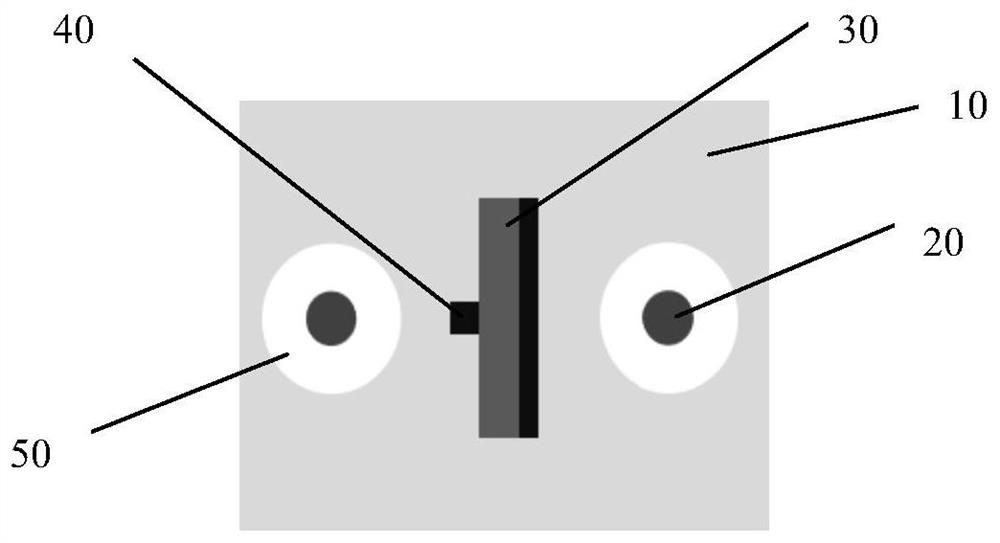
[0093] The selection of fiber raw materials includes PC particles with a diameter of about 3 mm for the fiber base material, and light-emitting diodes for the photoelectric chip. Specifically, the AlGaInP red light-emitting diode from ES-SABRPN14D of EPISTAR Company in Taiwan, China, with a wavelength of 660 nm and a chip size of 340μm×340μm×170μm, there are electrical contacts on opposite sides of the chip, and the lead wire is a tungsten wire with a wire diameter of 50μm.

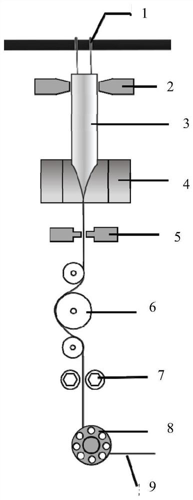
[0094] The preparation of the prefabricated part includes the following steps: put the fiber base material, that is, PC particles with a diameter of about 3mm, into the mold. The mold is 100mm long, 10mm wide, and 20mm high. The mold is a stainless steel groove, and special Teflon film coating prevents the heat-softened polymer material from sticking to the mold. The upper and lower sides of th...

Embodiment 2

[0099] The photoelectric chip integrated fiber prepared by the thermal stretching method in Example 2 of the present invention has red light and infrared light emitting functions.

[0100] The selection of fiber raw materials is as follows: PC particles with a diameter of about 3 mm are selected as the fiber base material; and a thin PC layer with a length of 100 mm, a width of 5 mm, and a height of 20 mm. There are two types of light-emitting diodes, which are AlGaInP red light-emitting diodes from ES-SABRPN14D of EPISTAR Company in Taiwan, China, with a wavelength of 660nm and a chip size of 340μm×340μm×170μm, with electrical contacts on opposite sides of the chip; The ES-SAUFPN08 AlGaAs infrared light-emitting diode of Taiwan EPISTAR Company has a wavelength of 940nm and a chip size of 185 μm × 185 μm × 150 μm. The lead wire is a tungsten wire with a wire diameter of 50 μm.

[0101] Put PC particles with a diameter of about 3mm into the mold. The length of the mold is 100m...

Embodiment 3

[0109] The optoelectronic chip integrated fiber prepared in this embodiment has the functions of red and green light emission.

[0110] The selection of fiber raw materials includes that PC particles with a diameter of about 3 mm are selected as the fiber base material. Two types of light-emitting diodes are selected for the optoelectronic chip. One type of light-emitting diode is an AlGaInP red light-emitting diode from ES-SABRPN14D of EPISTAR Company in Taiwan, China, with a wavelength of 660nm and a chip size of 340μm×340μm×170μm. point; Another option is the InGaN green light-emitting diode from ES-EEGHA09A of EPISTAR Company in Taiwan, China, with a wavelength of 525nm, a chip size area of ​​210μm×210μm, and a thickness of 110μm. The lead wire is a tungsten wire with a wire diameter of 50 μm.

[0111] Put PC particles with a diameter of about 3mm into the mold. The length of the mold is 100mm, the width is 10mm, and the height is 20mm. Die sticking. The upper and lower...


PUM

PropertyMeasurementUnit
thicknessaaaaaaaaaa
diameteraaaaaaaaaa
diameteraaaaaaaaaa

Abstract

The invention discloses a photoelectric chip integrated fiber manufacturing method, and fiber, yarn and fabric thereof. The manufacturing method comprises the following steps: a preform is manufactured from a fiber substrate material; a photoelectric chip and a lead are arranged in the preform, the preform is subjected to thermal stretching, so that the lead is in electric contact with the photoelectric chip in the thermal stretching process, a photoelectric chip integrated fiber is obtained, and the lead and the photoelectric chip keep fixed in form and performance in the thermal stretching process; or the lead is electrically connected with the photoelectric chip before thermal stretching, and further packaging is carried out through thermal stretching to form the photoelectric chip integrated fiber. The manufacturing method of the photoelectric chip integrated fiber, the fiber, the yarn and the fabric provided by the invention can be applied to the fields of omnibearing light emitting, gesture recognition, visual feedback, physiological monitoring and the like.

Description

technical field [0001] The invention relates to a method for making a fiber, in particular to a method for making a photoelectric chip integrated fiber and corresponding fiber products. Background technique [0002] With the development of composite materials and people's demand for intelligent life, as well as the vigorous development of the field of functional fibers in recent years, various functional fibers have been manufactured, such as conductive fibers, thermal fibers, magnetic control fibers, etc. In addition, scientists have combined it with textiles and applied it to the field of smart wearables to realize various functions such as communication, physiological monitoring, temperature regulation, and flexible lighting. [0003] Traditional wearable devices are produced on hard substrates. Functional devices are attached to the surface of the fabric, which will affect the comfort of the user. However, building fiber-based devices and combining them with textiles not...

Claims


Application Information

Patent Timeline
Patent Type & Authority Applications(China)
IPC IPC(8): H01L33/48H01L33/62D02G3/44D03D1/00D04B1/14D04B21/00D04H1/40D01F6/64
CPCH01L33/483H01L33/62D02G3/441D03D1/0088D04B1/14D04B21/00D04H1/40D01F6/64
Inventor 陶光明赵淑雅李攀侯冲张诚
Owner HUAZHONG UNIV OF SCI & TECH
Why Eureka
Try Eureka