Preparation method and application of hafnium nitride film with high crystal quality

A thin film preparation, hafnium nitride technology, applied in ion implantation plating, metal material coating process, coating and other directions, can solve the problems of slow growth rate of ALD material, low heating temperature of substrate, no test results, etc. Achieve the effect that is beneficial to the preparation of low stress and high crystalline quality, the improvement of film density and surface flatness, and the high film deposition growth rate

Active Publication Date: 2021-05-25
NANJING YOUTIAN METAL TECH +1
View PDF9 Cites 5 Cited by
  • Summary
  • Abstract
  • Description
  • Claims
  • Application Information

AI Technical Summary

Problems solved by technology

Among them, the growth rate of ALD materials is slow. Although high-purity HfN films with nanoscale thickness can be prepared, due to the low growth temperature, only amorphous or polycrystalline materials with poor crystal quality can be grown.
However, the preparation and growth of HfN thin films by MOCVD is still in research and development, and it has not been possible to realize the HfN (111) diffraction peak X-ray rocking curve (XRC) full width at half maximum (FWHM) on Si substrates down to a height below 1°. Quality Single Crystal Thin Film Growth Results Report
The Institute of Semiconductors of the Chinese Academy of Sciences has used ion beam epitaxy (IBE) to grow HfN thin films with a single preferred orientation. However, due to the small film area (2cm×2cm) of ion beam epitaxy, it is not suitable for the production of semiconductor devices. device
At present, magnetron sputtering is still the main process for preparing and growing HfN thin films, but most of the existing research results are not conducive to the formation of HfN due to the incomplete removal of the residual oxide layer on the surface of the Si substrate or the avoidance of the nitriding of the Si substrate surface first. Nucleated and grown amorphous Si x N y layer, or due to the relatively low heating temperature of the substrate or the relatively high sputtering power, most of the HfN thin films have not grown on the Si substrate with a single preferred orientation and high crystal quality. Most research results only obtain HfN polycrystalline thin films with disordered orientation, Surface relief is also large (AFM surface roughness (RMS) higher than 3nm)
Even if there is a result of achieving a single preferred orientation growth, there is no X-ray rocking curve (XRC) full width at half maximum (FWHM) test result that characterizes the thin film material as having single crystal quality

Method used


Image

  • Preparation method and application of hafnium nitride film with high crystal quality
  • Preparation method and application of hafnium nitride film with high crystal quality
  • Preparation method and application of hafnium nitride film with high crystal quality

Examples


Embodiment 1

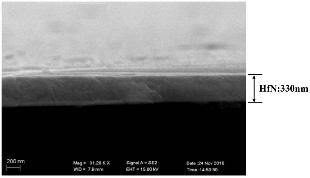
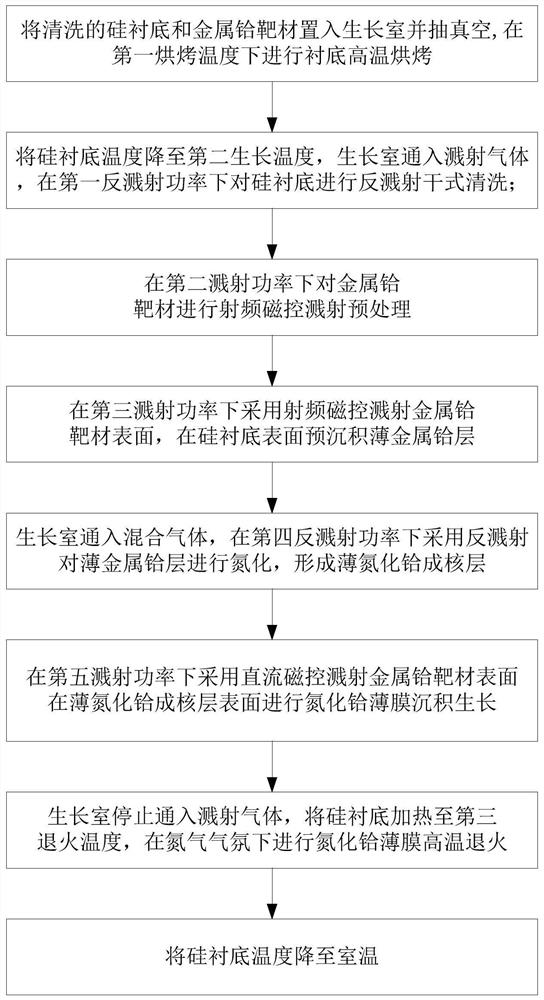
[0037] The invention discloses a method for preparing a hafnium nitride thin film with high crystal quality, such as figure 1 shown, including:

[0038] S1. Put the cleaned silicon substrate and metal hafnium target into the growth chamber of the magnetron sputtering equipment and evacuate to ultra-high vacuum, heat the silicon substrate to the first baking temperature, and perform ultra-high vacuum on the silicon substrate Baking under high temperature conditions;

[0039]The silicon substrate is a silicon single crystal substrate whose crystal orientation is not limited to (111), (100), (110) and (113), the size is not less than 1 inch in diameter, and the purity of the metal hafnium target is not less than 99.99%. In this embodiment, a 2-inch Si(111) substrate and a metal hafnium target with a diameter of 83 mm and a purity of 99.99% are used. The distance between the silicon substrate and the metal hafnium target is 5 to 15 cm. In this embodiment, the distance between th...

Embodiment 2

[0054] Embodiment 2 is the same as the method for preparing hafnium nitride thin film in embodiment 1, the difference is:

[0055] In step S1, the distance between the silicon substrate and the metal hafnium target is 5 cm; at the first baking temperature of 700° C., the silicon substrate is subjected to ultra-high vacuum and high-temperature baking surface treatment for 40 minutes to remove the particles adsorbed on the surface of the silicon substrate. Gas and residual impurities and oxide layer;

[0056] In step S2, the second growth temperature is 350°C, and the rotation speed of the substrate tray for the substrate rotation is 120 revolutions per minute; the low-energy argon ions generated by the sputtering gas argon ignition discharge are used for the first reverse sputtering power of 200W. Reverse sputtering dry cleaning on the surface of the silicon substrate for 3 minutes to completely remove the remaining impurities and oxide layer on the surface of the silicon subst...

Embodiment 3

[0064] Embodiment 3 is the same as the method for preparing hafnium nitride thin film in embodiment 1, the difference is:

[0065] In step S1, the distance between the silicon substrate and the metal hafnium target is 15 cm; at the first baking temperature of 850° C., carry out ultra-high vacuum high-temperature baking surface treatment of the silicon substrate for 15 minutes to remove the adsorbed particles on the surface of the silicon substrate. Gas and residual impurities and oxide layer;

[0066] In step S2, the second growth temperature is 650°C, and the rotation speed of the substrate tray on which the substrate rotates is 5 revolutions per minute; the low-energy argon ions generated by the sputtering gas argon initiation discharge are used at the first reverse sputtering power of 100W. Reverse sputtering dry cleaning on the surface of the silicon substrate for 20 minutes to completely remove the remaining impurities and oxide layer on the surface of the silicon substra...


PUM

PropertyMeasurementUnit
surface roughnessaaaaaaaaaa
diameteraaaaaaaaaa

Abstract

The invention discloses a preparation method of a hafnium nitride film with high crystal quality. The preparation method comprises the steps that 1, a silicon substrate is baked at a high temperature; 2, the temperature of the silicon substrate is reduced, sputtering gas argon is introduced, and reverse sputtering dry cleaning is carried out on the silicon substrate under first reverse sputtering power; 3, radio frequency magnetron sputtering pretreatment is carried out on a metal hafnium target material under second sputtering power; 4, a thin metal hafnium layer is pre-deposited on the surface of the silicon substrate by adopting radio frequency magnetron sputtering under third sputtering power; 5, reaction gas nitrogen and sputtering gas argon are introduced to form mixed gas, and a thin hafnium nitride nucleating layer is formed by adopting reverse sputtering under fourth reverse sputtering power; 6, hafnium nitride film deposition and growth are carried out by adopting direct-current magnetron sputtering under fifth sputtering power; 7, sputtering gas argon introducing is stopped, and high-temperature annealing is carried out on the hafnium nitride film in a nitrogen atmosphere; and 8, the temperature of the silicon substrate is reduced to room temperature. By means of the method, the hafnium nitride film with high crystal quality can be prepared on the silicon substrate.

Description

technical field [0001] The invention belongs to the technical field of semiconductor and thin film material preparation, and in particular relates to a method for preparing a hafnium nitride thin film on a silicon substrate by magnetron sputtering. Background technique [0002] Transition group refractory metal nitrides (including: titanium nitride (TiN), zirconium nitride (ZrN), hafnium nitride (HfN)) usually have a cubic rock-salt structure, which not only has good thermal and chemical stability, but also has good The electrical conductivity and resistivity are even comparable to some metal materials with good electrical conductivity. In the field of semiconductor technology, especially silicon-based device technology, transition group refractory metal nitride thin film materials have extremely important application value. For example, the magnetron sputtering and atomic layer deposition preparation processes of TiN films are relatively mature, and are the most commonly u...

Claims


Application Information

Patent Timeline
Patent Type & Authority Applications(China)
IPC IPC(8): C23C14/35C23C14/16C23C14/06C23C14/02C23C14/58C23C14/54
CPCC23C14/35C23C14/165C23C14/0036C23C14/0641C23C14/022C23C14/5806C23C14/54
Inventor 魏洁陈怀浩杨少延魏鸿源高洁
Owner NANJING YOUTIAN METAL TECH
Why Eureka
Try Eureka