Wafer manufacturing process for preparing ILD insulating layer by using low-frequency radio-frequency plasma
A manufacturing process and insulating layer technology, which is applied in metal material coating process, semiconductor/solid-state device manufacturing, coating, etc., can solve the problems of unstable bonding of dopants, gaps in the process, and difficult solutions, and achieve the goal of doping Stable bonding of impurities, good adsorption effect, and high reliability
- Summary
- Abstract
- Description
- Claims
- Application Information
AI Technical Summary
Problems solved by technology
Method used
Image
Examples
Embodiment 1
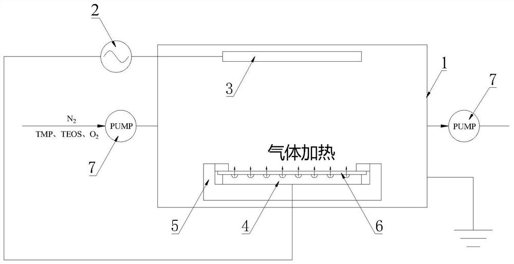
[0032] A wafer manufacturing process utilizing low-frequency radio-frequency plasma to prepare an ILD insulating layer, comprising the following steps:
[0033] S1. After cleaning the surface of the wafer, put it into the RF plasma reactor, fix the edge of the wafer with a ring clamp, inject high-temperature gas from the gap of the lower electrode to heat the bottom of the wafer, and keep the wafer at 450°C;
[0034] S2, the RF plasma reactor is evacuated by a vacuum pump, so that the inside of the RF plasma reactor is in a vacuum state, and then N 2 Reaching the reaction pressure is 200mTorr;
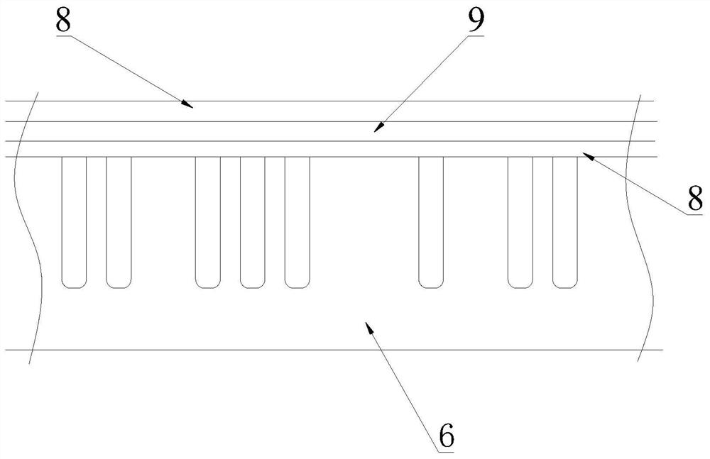
[0035] S3, access to TEOS and O 2 At the same time, the distance between the electrode plates is controlled, the RF power is turned on, and the plasma is generated between the electrodes through the bombardment of 800KHz low-frequency RFgenerate to deposit the ILD-1 layer on the wafer surface; then TEOS, TMP and O 2 , Deposit the ILD-2 layer on the surface of the ILD-1 layer by 800KH...
Embodiment 2
[0037] A wafer manufacturing process utilizing low-frequency radio-frequency plasma to prepare an ILD insulating layer, comprising the following steps:
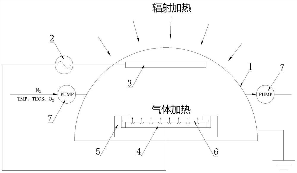
[0038] S1. Clean the surface of the wafer and put it into the RF plasma reactor. The edge of the wafer is fixed with a ring fixture, and high-temperature gas is injected from the gap of the lower electrode to heat the bottom of the wafer combined with radiation heating to keep the wafer at 550°C;
[0039] S2, the RF plasma reactor is evacuated by a vacuum pump, so that the inside of the RF plasma reactor is in a vacuum state, and then N 2 Reaching the reaction pressure is 50mTorr;
[0040] S3, access to TEOS and O 2 At the same time, the distance between the electrode plates is controlled, the RF power is turned on, and the plasma is generated between the electrodes through the bombardment of 500KHz low-frequency RFgenerate to deposit the ILD-1 layer on the wafer surface, and then TEOS, TMP and O 2 , deposit the ILD-2 layer...
PUM
 Abstract
Description
Claims
Application Information
 - R&D
- Intellectual Property
- Life Sciences
- Materials
- Tech Scout
- Unparalleled Data Quality
- Higher Quality Content
- 60% Fewer Hallucinations
Browse by: Latest US Patents, China's latest patents, Technical Efficacy Thesaurus, Application Domain, Technology Topic, Popular Technical Reports.
© 2025 PatSnap. All rights reserved.Legal|Privacy policy|Modern Slavery Act Transparency Statement|Sitemap|About US| Contact US: help@patsnap.com


