Preparation device and preparation process of electronic film material
An electronic thin film and preparation device technology, applied in metal material coating process, gaseous chemical plating, coating and other directions, can solve the problems of difficult realization of thin film, high energy consumption of thin film, low film forming efficiency, etc. The effect of uniformity, high growth rate and good adsorption effect
- Summary
- Abstract
- Description
- Claims
- Application Information
AI Technical Summary
Problems solved by technology
Method used
Image

Examples
Embodiment 1
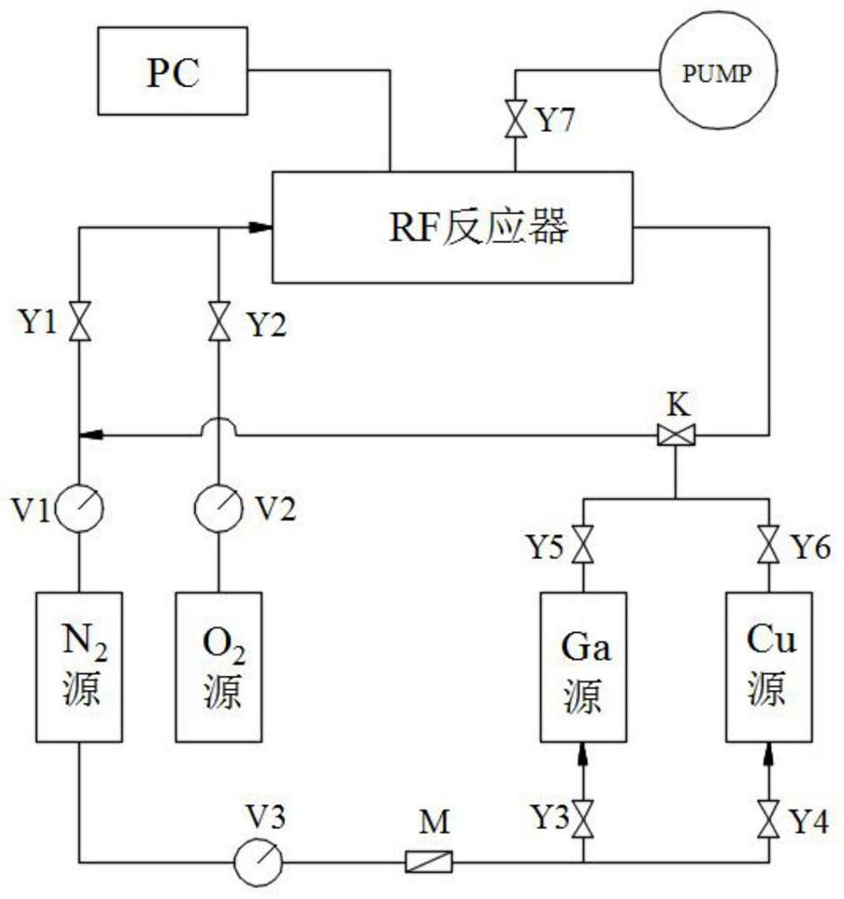
[0048] A preparation process for an electronic thin film material, specifically comprising the following steps:
[0049] S1. Immerse the silicon wafer substrate in acetone, absolute ethanol, and deionized water for 8 minutes for ultrasonic cleaning, then rinse with deionized water after taking it out, and finally wash it with dry N 2 Blow dry and set aside;
[0050] S2. Fix the silicon wafer substrate on the sample holder, then close the cover plate of the deposition chamber, evacuate the deposition chamber to a vacuum degree of 5Pa by an air pump, and then fill the deposition chamber with N 2 To standard atmospheric pressure, turn on the substrate heating device to heat the substrate to 85°C;
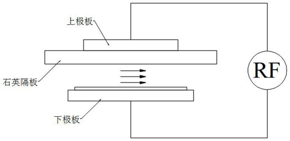
[0051] S3. Control the distance between the electrode plates to 7mm, turn on the RF power supply, the RF frequency is 450KHz, and the RF power is 100W. 2 The organic gallium precursor Ga(CH 3 ) 3 brought into the deposition chamber, the organic gallium precursor Ga(CH 3 ) 3 The a...
Embodiment 2
[0057] A preparation process for an electronic thin film material, specifically comprising the following steps:
[0058] S1. Immerse the PET film substrate in acetone, absolute ethanol, and deionized water for 5 minutes for ultrasonic cleaning, then rinse it with deionized water after taking it out, and finally wash it with dry N 2 Blow dry and set aside;
[0059] S2. Fix the PET film substrate on the sample holder, then close the cover plate of the deposition chamber, evacuate the deposition chamber to a vacuum degree of 8Pa by an air pump, and then fill the deposition chamber with N 2 To standard atmospheric pressure, turn on the substrate heating device to heat the substrate to 80°C;
[0060] S3. Control the distance between the electrode plates to 6mm, turn on the RF power supply, the RF frequency is 800KHz, and the RF power is 150W. 2 The organic gallium precursor Ga(C 2 h 5 ) 3 brought into the deposition chamber, the organic gallium precursor Ga(C 2 h 5 ) 3 The ...
Embodiment 3
[0065] A preparation process for an electronic thin film material, specifically comprising the following steps:
[0066] S1. Submerge the potassium bromide tablet substrate into acetone, absolute ethanol, and deionized water for 8 minutes to ultrasonically clean it, then rinse it with deionized water after taking it out, and finally wash it with dry N 2 Blow dry and set aside;
[0067] S2. Fix the potassium bromide sheet substrate on the sample holder, then close the cover plate of the deposition chamber, vacuum the deposition chamber to a vacuum degree of 5Pa by an air pump, and then fill the deposition chamber with N 2 To standard atmospheric pressure, turn on the substrate heating device to heat the substrate to 90°C;
[0068] S3. Control the distance between the electrode plates to 7mm, turn on the RF power supply, the RF frequency is 500KHz, and the RF power is 50W. 2 The organogallium precursor C 9 h 21 GaO 3 brought into the deposition chamber, the organic gallium ...
PUM
 Abstract
Description
Claims
Application Information
 - R&D
- Intellectual Property
- Life Sciences
- Materials
- Tech Scout
- Unparalleled Data Quality
- Higher Quality Content
- 60% Fewer Hallucinations
Browse by: Latest US Patents, China's latest patents, Technical Efficacy Thesaurus, Application Domain, Technology Topic, Popular Technical Reports.
© 2025 PatSnap. All rights reserved.Legal|Privacy policy|Modern Slavery Act Transparency Statement|Sitemap|About US| Contact US: help@patsnap.com