Superlattice Gradient Band-Hole Barrier Layer Structure and Infrared Detector
A technology of infrared detectors and superlattice layers, applied in semiconductor devices, electrical components, circuits, etc., can solve problems affecting the optical and electrical performance of infrared detection devices, poor controllability of interface quality, and reduced material quality. The effect of large band offset, meeting the design requirements, and small conduction band offset
- Summary
- Abstract
- Description
- Claims
- Application Information
AI Technical Summary
Problems solved by technology
Method used
Image
Examples
Embodiment 1
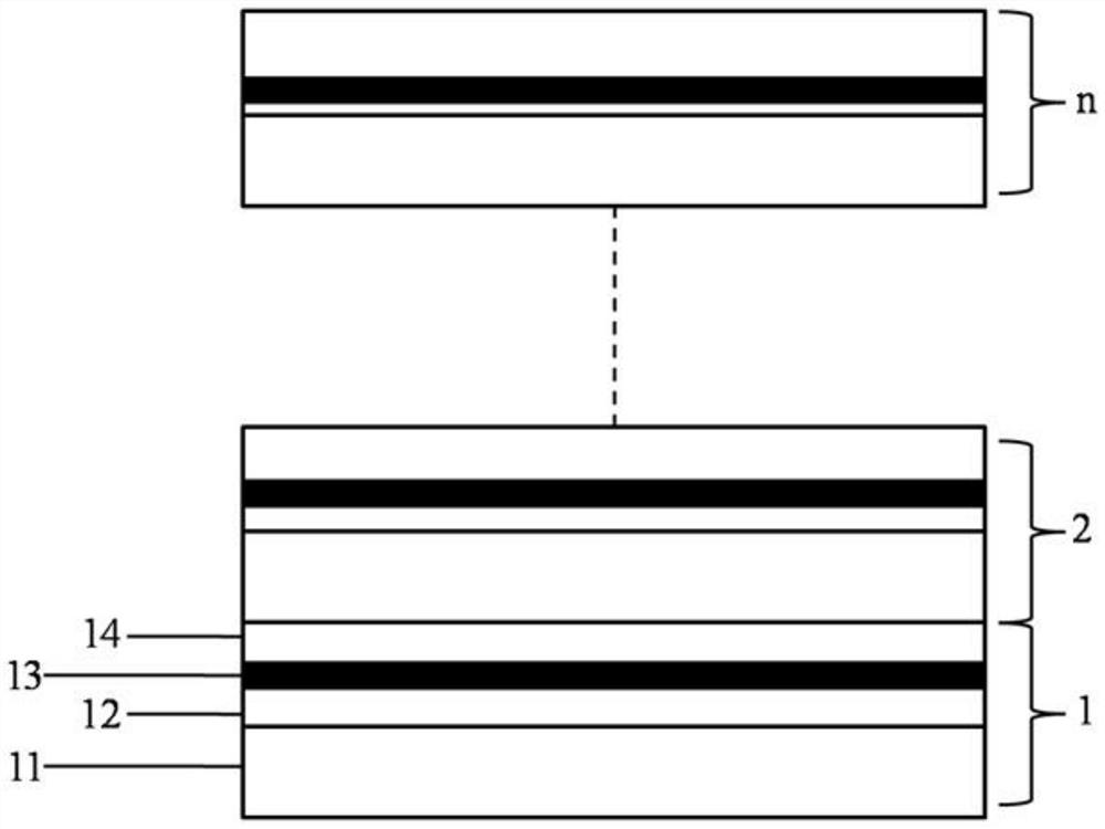
[0025] Embodiment 1: A superlattice gradient energy band hole barrier layer structure, its specific structure from bottom to top is as follows:
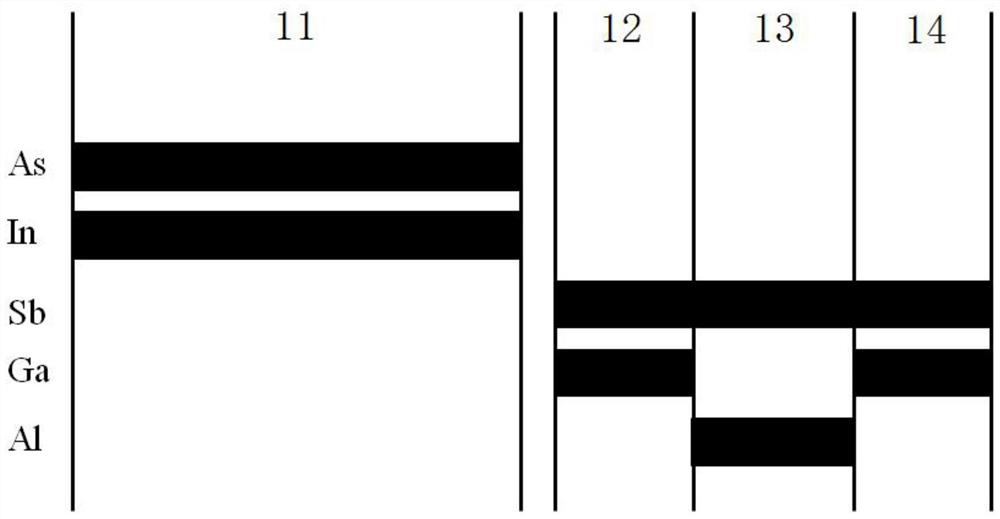
[0026] The first-level superlattice, with a period number of 5, is composed of 5.4nm InAs, 0.9nm GaSb, 1.5nm AlSb and 0.9nm GaSb layers, and the period thickness is 8.7nm;
[0027] The second-level superlattice, with a period number of 5, consists of 5.4nm InAs, 0.6nm GaSb, 1.5nm AlSb and 1.2nm GaSb layers, with a period thickness of 8.7nm;
[0028] The third-level superlattice, with a period number of 5, is composed of 5.4nm InAs, 0.3nm GaSb, 1.5nm AlSb and 1.5nm GaSb layers, and the period thickness is 8.7nm;
[0029] The fourth-level superlattice, with a period number of 5, consists of 5.4nm InAs, 0nm GaSb, 1.5nm AlSb and 1.8nm GaSb layers, with a period thickness of 8.7nm.
[0030] According to the analysis and calculation of the energy band theory, the energy band gap of the hole barrier layer of this structure increases from 0...
Embodiment 2
[0031] Embodiment 2: A superlattice gradient energy band hole barrier layer structure, its specific structure from bottom to top is as follows:
[0032] The first-level superlattice, with a period number of 10, is composed of 5.7nm InAs, 0.6nm GaSb, 1.8nm AlSb and 0.6nm GaSb layers, and the period thickness is 8.7nm;
[0033] The second-level superlattice, with a period of 10, consists of 5.7nm InAs, 0.3nm GaSb, 1.8nm AlSb and 0.9nm GaSb layers, with a period thickness of 8.7nm;
[0034]The third-level superlattice, with a period of 10, consists of 5.7nm InAs, 0nm GaSb, 1.8nm AlSb and 1.2nm GaSb layers, with a period thickness of 8.7nm.
[0035] According to the analysis and calculation of the energy band theory, the energy band of the hole barrier layer of this structure increases from 0.3450eV to 0.5268eV step by step from the first-level superlattice, and the corresponding conduction band offset is 0.002 eV, and the valence band offset is 0.1838eV, fully meeting the design...
PUM
 Abstract
Description
Claims
Application Information
 - R&D
- Intellectual Property
- Life Sciences
- Materials
- Tech Scout
- Unparalleled Data Quality
- Higher Quality Content
- 60% Fewer Hallucinations
Browse by: Latest US Patents, China's latest patents, Technical Efficacy Thesaurus, Application Domain, Technology Topic, Popular Technical Reports.
© 2025 PatSnap. All rights reserved.Legal|Privacy policy|Modern Slavery Act Transparency Statement|Sitemap|About US| Contact US: help@patsnap.com


