Anticorrosive coating for nano metal and preparation method of anticorrosive coating
An anti-corrosion coating and nano-metal technology, which is applied in the direction of anti-corrosion coatings, coatings, and devices for coating liquid on the surface, can solve the problems of unfavorable long-term and effective protection of metal nano-materials, and achieve long-term stability and little impact on physical properties , cost-effective effect
- Summary
- Abstract
- Description
- Claims
- Application Information
AI Technical Summary
Problems solved by technology
Method used
Image
Examples
Embodiment 1
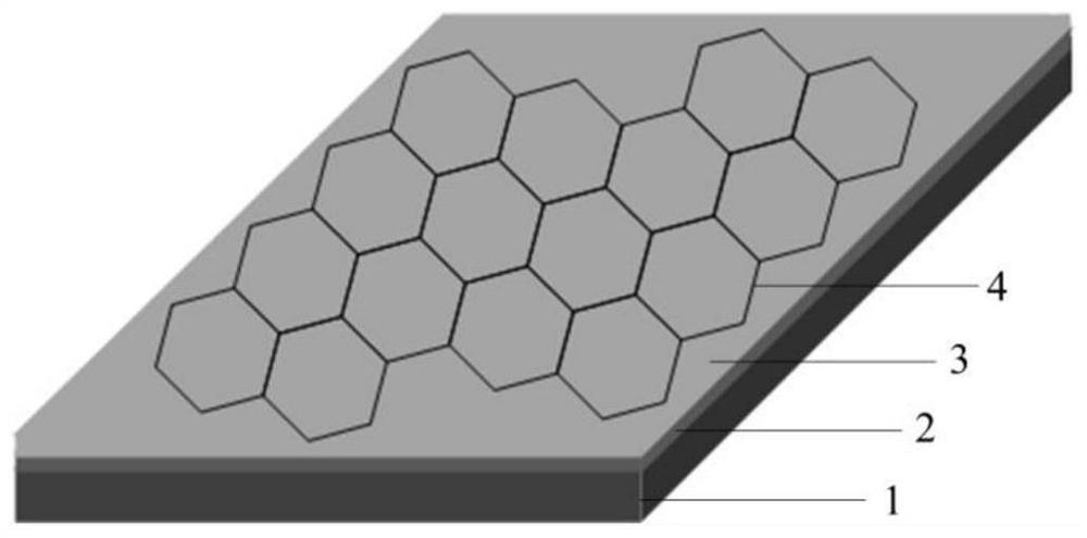
[0021] Copper nano film—PVP—hBN: Copper nano film with a thickness of 60nm was prepared by electron beam evaporation coating method. up to 1×10 -7 At bar, the film growth rate was controlled at ~2A / s, and the thickness of the evaporated film was monitored by a calibrated quartz microcrystal balance. It should be noted that before copper plating, a 1.5nm thick chromium film (film growth rate: ~0.6A / s) needs to be evaporated on the glass substrate to be used as an adhesive between the glass substrate and the copper film . Then the high polymer PVP (2%PVP, solvent: deionized water, PVP molecular weight: 1300000) coating spin-coating with thickness less than 20nm is placed on the surface of the above-mentioned copper nano film structure, wherein the spin-coating speed is 6000r / min, spin-coating The time is 2 minutes. Finally, the 1 × 1 cm 2 The specific process is as follows: firstly, the PMMA solution is spin-coated on the iron foil surface with hBN grown by CVD method, and t...
Embodiment 2
[0023] Silver nanowires-PMMA-bilayer graphene: First, the silver nanowire structure is placed on the surface of a clean silicon wafer substrate. Then, a polymer PMMA (0.1% PMMA, solvent: chlorobenzene) coating with a thickness of less than 10 nm was spin-coated on the surface of the silver nanowire structure, and baked at 120° C. for 3 minutes. Wherein the spin coating speed is 8000r / min, and the spin coating time is 2min. Finally, the 1×1cm 2 The single-layer CVD graphene of the above-mentioned silver nanowire structure surface is transferred to the surface of the above-mentioned silver nanowire structure. 2 , cleaning time: 20s) to remove pollutants and oxides on the back of the copper foil (the side without graphene); then use 25g / l ammonium persulfate solution to etch off the copper foil; use deionized water to wash the attached Graphene with PMMA; then transfer it to the silver nanowire structure surface containing high polymer PMMA coating, after drying at 120 ° C for ...
Embodiment 3
[0025] Silver nanofilm—PDMS—double-layer hBN: A silver nanofilm with a thickness of 50nm was prepared by electron beam evaporation coating method. Bulk vacuum up to 1×10 -7 At bar, the film growth rate was controlled at ~5A / s, and the thickness of the evaporated film was monitored by a calibrated quartz microcrystal balance. It should be noted that before the silver coating, a 1.5nm thick chromium film (film growth rate: ~0.6A / s) needs to be evaporated on the glass substrate to be used as an adhesive between the glass substrate and the silver film . Then the high polymer PDMS with thickness less than 20nm (using silicone oil to dilute PDMS (the mass ratio of silicone oil and PDMS is 1:1)) coating is spin-coated and placed on the surface of the above-mentioned silver nano film structure, wherein the spin-coating speed is 8000r / min, Spin coating time is 2min. Finally, the 1×1cm 2 The specific process is as follows: firstly, the PMMA solution is spin-coated on the surface of ...
PUM
| Property | Measurement | Unit |
|---|---|---|
| Thickness | aaaaa | aaaaa |
Abstract
Description
Claims
Application Information
 - R&D
- Intellectual Property
- Life Sciences
- Materials
- Tech Scout
- Unparalleled Data Quality
- Higher Quality Content
- 60% Fewer Hallucinations
Browse by: Latest US Patents, China's latest patents, Technical Efficacy Thesaurus, Application Domain, Technology Topic, Popular Technical Reports.
© 2025 PatSnap. All rights reserved.Legal|Privacy policy|Modern Slavery Act Transparency Statement|Sitemap|About US| Contact US: help@patsnap.com

