


Quick Research
Generate reliable direction feasibility study reports for your R&D in just a few steps.

Technical Q&A
Discover and master advanced knowledge NOW. Basics, ideas, possibilities, all at once.

Find Solutions
As an expert in R&D theories, this can generate solutions to your technical problems instantly.

Evaluate Feasibility
Analyze your overall solution with one click, know your potential R&D risks in advance.

Monitor Landscape
Get weekly tech updates, stay abreast of the latest tech innovations and key insights.
Mini LED chip structure and manufacturing method thereof
A chip structure and chip technology, applied in electrical components, circuits, semiconductor devices, etc., can solve problems such as metal layer migration, and achieve the effects of excellent high temperature resistance, stable process window, and good resistance to electromigration.
- Summary
- Abstract
- Description
- Claims
- Application Information
AI Technical Summary
Problems solved by technology
Method used
Image

Examples
Embodiment 1
[0051] Please refer to Figure 1 to Figure 3 , Embodiment 1 of the present invention is:
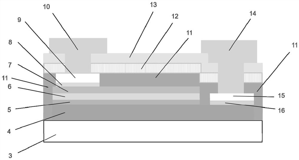
[0052] A Mini LED chip structure, please refer to figure 1 , including:
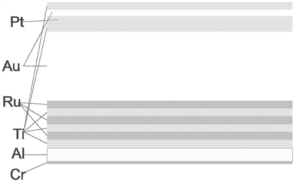
[0053] Substrate layer 3, N-type gallium nitride layer 4, multi-layer quantum well layer 5, P-type gallium nitride layer 6, current spreading layer 7, first current stabilizing layer 8, P-type current spreading injection metal layer 9, P-type Welding interface metal layer 10, second current stabilization layer 16, N-type current expansion injection metal layer 15, N-type welding interface metal layer 14, buffer insulating layer 11, stress release layer 12 and insulating full-spectrum reflective layer 13;
[0054] The N-type gallium nitride layer 4 is located in the middle area on one side of the substrate layer 3, and the side of the Mini LED chip close to the other side of the substrate layer 3 is the bottom of the Mini LED chip; The first stacked area on one side of one side is sequentially stacked with a mult...
Embodiment 2
[0060] Please refer to Figure 4 , the second embodiment of the present invention is:
[0061] A method for manufacturing a Mini LED chip, specifically comprising:
[0062] S1. Transfer the prepared GaN epitaxial material according to the first preset pattern through photolithography facilities, and then use ICP equipment to etch the GaN epitaxial wafer to form an N-type GaN layer on the substrate;
[0063] S2. First, make a current spreading layer template through an evaporation machine or a sputtering machine. The material of the current spreading layer template can be indium tin oxide, indium tungsten oxide, nickel-gold alloy, etc., and then use photolithography facilities to make the current spreading layer template Perform pattern transfer according to the second preset pattern, and finally corrode the current spreading layer template by chemical reagents to form a current spreading layer;
[0064] Chemical reagents can be hydrochloric acid, oxalic acid, ferric chloride...
PUM
| Property | Measurement | Unit |
|---|---|---|
| Thickness | aaaaa | aaaaa |
Abstract
Description
Claims
Application Information
 - R&D Engineer
- R&D Manager
- IP Professional
- Industry Leading Data Capabilities
- Powerful AI technology
- Patent DNA Extraction
Browse by: Latest US Patents, China's latest patents, Technical Efficacy Thesaurus, Application Domain, Technology Topic, Popular Technical Reports.
© 2024 PatSnap. All rights reserved.Legal|Privacy policy|Modern Slavery Act Transparency Statement|Sitemap|About US| Contact US: help@patsnap.com