Single-sided texturing process of monocrystalline silicon wafer, and preparation method of solar cell
A monocrystalline silicon wafer, single-sided texturing technology, applied in the direction of single crystal growth, single crystal growth, chemical instruments and methods, etc., can solve the problem of poor passivation effect on the back of the battery sheet, unsatisfactory flatness of the back polished surface, Issues affecting the quality of monocrystalline PERC cells
- Summary
- Abstract
- Description
- Claims
- Application Information
AI Technical Summary
Problems solved by technology
Method used
Image
Examples
preparation example Construction
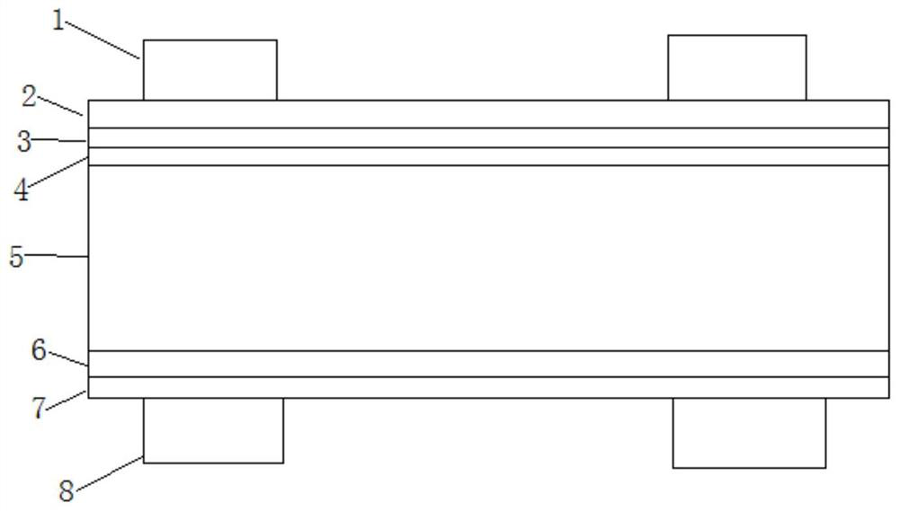
[0051] The present invention also provides a method for preparing a solar cell, comprising the following steps:
[0052] 1) Prepare a phosphorous diffusion layer and a silicon dioxide tunneling layer sequentially on the front side of the above-mentioned front textured monocrystalline silicon wafer,
[0053] 2) depositing an aluminum oxide layer on the back side of the monocrystalline silicon wafer obtained in the step 1);
[0054] 3) depositing a silicon nitride layer with a thickness of 60 to 90 nm on the front side of the monocrystalline silicon wafer obtained in step 2);
[0055] 4) Depositing a silicon nitride layer with a thickness of 100-150 nm on the back side of the monocrystalline silicon wafer obtained in step 3)
[0056] 5) performing laser drilling on the back of the monocrystalline silicon wafer obtained in step 4), and then sintering the screen to obtain a solar cell.
[0057] The present invention carries out phosphorus diffusion on the textured surface (i.e. ...
Embodiment 1
[0068] Add resin, cellulose, additives, and nano-silica powder in a certain proportion, heat and stir at 60°C for 5 minutes, and prepare a solution-like colloid (mass ratio of silica powder: additive: cellulose: resin = 1:1:0.5: 15.
[0069] Place the P-type monocrystalline silicon wafer on the tray of the spin-coating instrument, drop mask glue on the back surface of the silicon wafer, and spin-coat to prepare a mask glue with a thickness of 2 μm;
[0070] For texturing, use potassium hydroxide solution for texturing, and use 10% HF aqueous solution to wash off the mask glue after texturing;
[0071] Phosphorus diffusion to obtain a phosphorus diffusion layer with a square resistance of 130Ω / □ to form an N+ emitter;
[0072] Use etching equipment to remove phospho-silicate glass and polish the back surface; since the back surface does not participate in the texturing reaction, no pyramid-like texture is formed, and the back surface is relatively flat compared with convention...
Embodiment 2
[0080] Add resin, cellulose, additives, and nano-silica powder in a certain proportion, heat and stir at 60°C for 5 minutes, and prepare a solution-like colloid (mass ratio of silica powder: additive: cellulose: resin = 0.5:1:0.5: 20.
[0081] Place the P-type monocrystalline silicon wafer on the tray of the spin-coating instrument, drop the mask glue on the back surface of the silicon wafer, and spin-coat to prepare a mask glue with a thickness of 1 μm;
[0082] For texturing, use potassium hydroxide solution for texturing, and use 10% HF aqueous solution to wash off the mask glue after texturing;
[0083] Phosphorus diffusion to obtain a phosphorus diffusion layer with a square resistance of 110Ω / □, forming an N+ emitter;
[0084] Use etching equipment to remove phospho-silicate glass and polish the back surface; since the back surface does not participate in the texturing reaction, no pyramid-like texture is formed, and the back surface is relatively flat compared with con...
PUM
| Property | Measurement | Unit |
|---|---|---|
| thickness | aaaaa | aaaaa |
| thickness | aaaaa | aaaaa |
| thickness | aaaaa | aaaaa |
Abstract
Description
Claims
Application Information
 - R&D
- Intellectual Property
- Life Sciences
- Materials
- Tech Scout
- Unparalleled Data Quality
- Higher Quality Content
- 60% Fewer Hallucinations
Browse by: Latest US Patents, China's latest patents, Technical Efficacy Thesaurus, Application Domain, Technology Topic, Popular Technical Reports.
© 2025 PatSnap. All rights reserved.Legal|Privacy policy|Modern Slavery Act Transparency Statement|Sitemap|About US| Contact US: help@patsnap.com

