Optical device of flexible implantable neural photoelectrode and its design and fabrication method
An optical device and design method technology, applied in the field of neuroscience, can solve the problems of large shear force and other stresses, difficult to achieve stable work, increase implantation damage and other problems, so as to reduce nerve scar and implantation damage. , to achieve high-density effect
- Summary
- Abstract
- Description
- Claims
- Application Information
AI Technical Summary
Problems solved by technology
Method used
Image
Examples
Embodiment 1
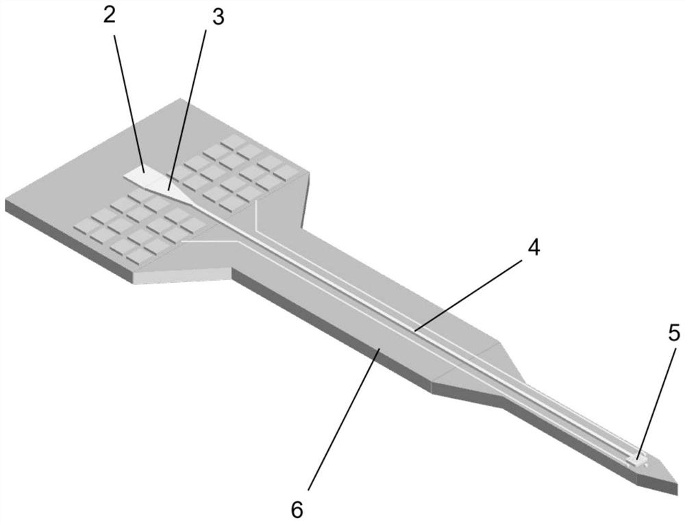
[0075] Embodiment 1 of the present invention provides an optical device of a flexible implantable neural photoelectrode, and the optical device 1 is disposed on a flexible polymer substrate 6 of the flexible implantable neural photoelectrode. The split structure of the flexible implantable neural photoelectrode is as follows: figure 1 shown. The bottom layer of the flexible implantable neural photoelectrode is an optical device 1, and the optical device 1 is arranged on a flexible polymer substrate 6, and the flexible polymer substrate 6 is made of a flexible polymer material.
[0076] The structure of the optical device 1 of the flexible implantable nerve photoelectrode is as follows figure 2 shown. The said optical device 1 comprises:
[0077] input grating 2, waveguide 4 and output grating 5,
[0078] The input grating 2 is a parallel grating structure for coupling incident light 9 with a preset wavelength and incident angle,
[0079] The input end of the waveguide 4 ...
Embodiment 2
[0085] Embodiment 2 of the present invention provides a design method for an optical device of a flexible and flexible implantable neural photoelectrode. The optical device 1 is arranged on a flexible polymer substrate 6 of a flexible implantable neural photoelectrode. The method includes:
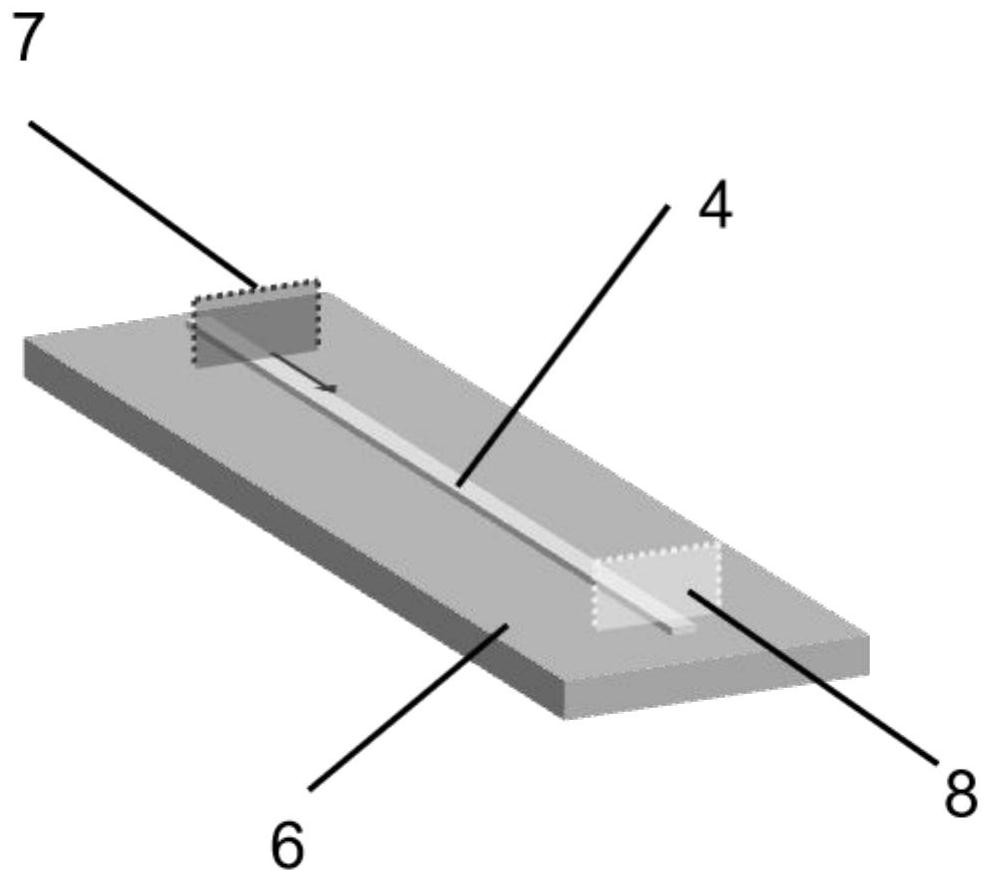
[0086] S100: Set up a mode light source 7 and a field monitor 8 on both sides of the waveguide 4, perform simulation based on the finite difference time domain method and determine the size parameters of the waveguide 4, and complete the design of the waveguide 4.
[0087] Specifically, such as image 3 and Figure 4 As shown, step S100 provided in Embodiment 2 of the present invention may include the following steps:
[0088] S110: Perform initial structure setting and parameter setting according to selected materials and process parameters, the parameter setting includes flexible polymer substrate refractive index, waveguide refractive index, waveguide size, waveguide surface roughness ...
Embodiment 3
[0125] Embodiment 3 of the present invention provides a method for preparing an optical device of a flexible implantable neural photoelectrode, such as Figure 12 As shown, the method includes:
[0126] S1: On a clean substrate, the photoresist is patterned by photolithography to obtain an alignment mark structure.
[0127] Preferably, the substrate is a single-polished silicon wafer with a thickness of 300-500 μm (for example, 400 μm), and the single-polished silicon wafer is cleaned and ready for use.
[0128] S2: Depositing metal on the patterned photoresist to obtain a metal alignment mark structure.
[0129] Specifically, on the patterned photoresist, a chromium / gold alloy layer with a thickness of 5nm / 50nm-10nm / 100nm (for example, 5nm / 100nm) is deposited by thermal evaporation, and the metal alignment is obtained by a lift-off process. markup structure.
[0130] S3: Prepare a flexible polymer substrate 6 by photolithography on the metal alignment mark structure prepar...
PUM
| Property | Measurement | Unit |
|---|---|---|
| thickness | aaaaa | aaaaa |
| surface roughness | aaaaa | aaaaa |
| thickness | aaaaa | aaaaa |
Abstract
Description
Claims
Application Information
 - R&D
- Intellectual Property
- Life Sciences
- Materials
- Tech Scout
- Unparalleled Data Quality
- Higher Quality Content
- 60% Fewer Hallucinations
Browse by: Latest US Patents, China's latest patents, Technical Efficacy Thesaurus, Application Domain, Technology Topic, Popular Technical Reports.
© 2025 PatSnap. All rights reserved.Legal|Privacy policy|Modern Slavery Act Transparency Statement|Sitemap|About US| Contact US: help@patsnap.com


