Novel high-current n-type TFET device with buried layer structure and preparation method thereof
A high-current, layer-structured technology, used in semiconductor/solid-state device manufacturing, electrical components, semiconductor devices, etc., can solve problems such as poor work function, increased device threshold voltage, etc.
- Summary
- Abstract
- Description
- Claims
- Application Information
AI Technical Summary
Problems solved by technology
Method used
Image

Examples
Embodiment 1
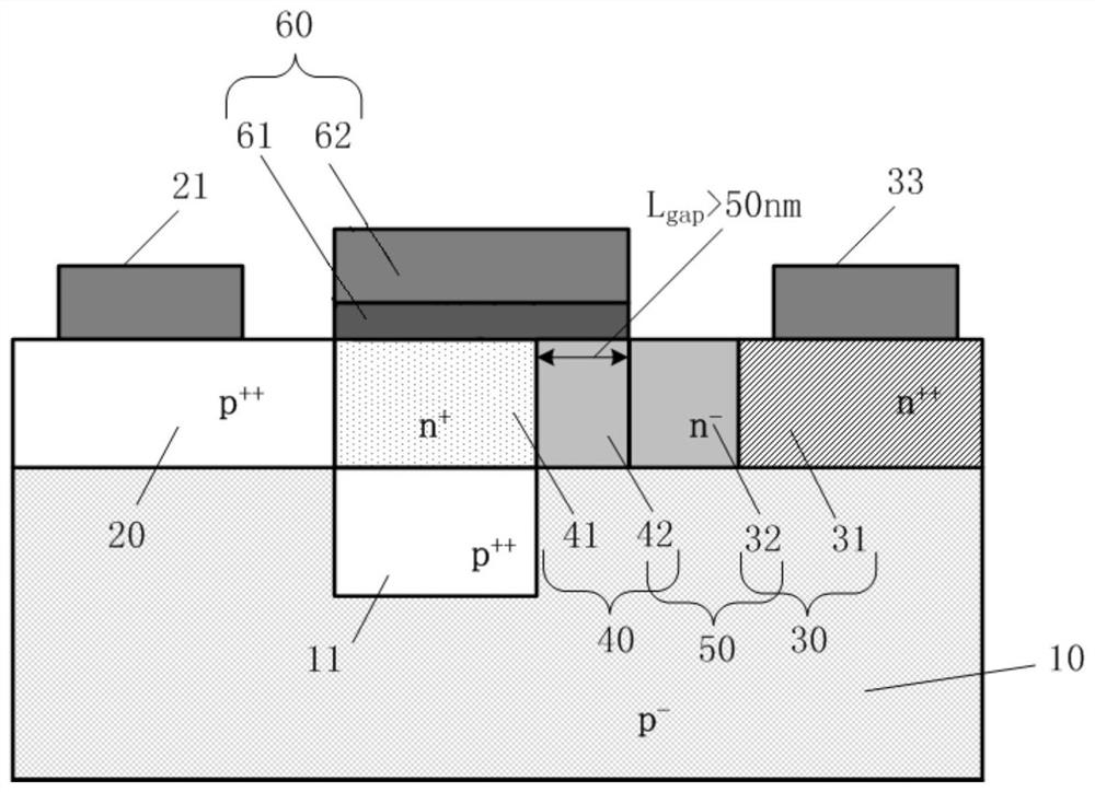
[0047] figure 1 It is a structural schematic diagram of a novel high-current n-type TFET device with a buried layer structure provided by an embodiment of the present invention, including:
[0048] Substrate 10;
[0049] The surface of the substrate 10 is provided with a source region 20 , a drain region 30 and a channel region 40 ; wherein the source region 20 and the drain region 30 are respectively located at both ends of the channel region 40 ;
[0050]A buried layer 11 is disposed under the channel region 40, the buried layer 11 starts at the junction of the channel region 40 and the source region 20, and the length of the buried layer 11 is shorter than that of the channel the length of zone 40;
[0051] A gate structure 60 is provided above the channel region 40; the gate structure 60 includes a gate electrode 62 and a gate dielectric layer 61 between the gate electrode 62 and the channel region 40;
[0052] A source electrode 21 and a drain electrode 33 are correspo...
Embodiment 2
[0074] On the basis of the first embodiment above, this embodiment provides a method for preparing a novel high-current n-type TFET device with a buried layer structure. Please refer to Figure 4 , Figure 4 It is a schematic diagram of a method for preparing a novel high-current n-type TFET device with a buried layer structure provided by an embodiment of the present invention, including:
[0075] S1: Get p with a certain doping concentration - substrate.
[0076] In this embodiment, the substrate material is lightly doped, and may be a single crystal Ge substrate, Si substrate or other substrate materials.
[0077] S2: In the p - heavily doped p ++ buried layer.
[0078] Specifically, a single crystal Ge substrate can be selected, and photolithography is performed to form a buried layer ion implantation window; ion doping is performed at a position corresponding to the buried layer to form a p-type buried layer; wherein, the buried layer and the substrate are doped with...
Embodiment 3
[0095] The device simulation parameters in the first embodiment are specifically taken below, and the manufacturing method of the present invention will be described in detail.
[0096] See Figure 5a~5h , Figure 5a~5h It is a schematic diagram of the preparation process of a novel high-current n-type TFET device with a buried layer structure provided by an embodiment of the present invention, including:
[0097] Step 1: Select a doping concentration of 1×10 17 cm -3 the p - Type single crystal Ge is the initial material, and it is used as the substrate 101, such as Figure 5a shown.
[0098] Step 2: Perform the first photolithography to form a buried layer ion implantation window in a specific region of the substrate 101; perform selective ion implantation on it, and anneal to activate impurities to form a doping concentration of 1×10 20 cm -3 , a thickness of 10nm P ++ type buried layer 102, such as Figure 5b shown.
[0099] Step 3: On the substrate with the bur...
PUM
| Property | Measurement | Unit |
|---|---|---|
| Doping concentration | aaaaa | aaaaa |
| Thickness | aaaaa | aaaaa |
Abstract
Description
Claims
Application Information
 - R&D
- Intellectual Property
- Life Sciences
- Materials
- Tech Scout
- Unparalleled Data Quality
- Higher Quality Content
- 60% Fewer Hallucinations
Browse by: Latest US Patents, China's latest patents, Technical Efficacy Thesaurus, Application Domain, Technology Topic, Popular Technical Reports.
© 2025 PatSnap. All rights reserved.Legal|Privacy policy|Modern Slavery Act Transparency Statement|Sitemap|About US| Contact US: help@patsnap.com