Semiconductor device and forming method thereof

A semiconductor and device technology, applied in the field of semiconductor devices and their formation, can solve problems such as photoresist residue, device leakage current, and high cost

Active Publication Date: 2020-10-02
SEMICON MFG ELECTRONICS (SHAOXING) CORP +1
View PDF5 Cites 2 Cited by
  • Summary
  • Abstract
  • Description
  • Claims
  • Application Information

AI Technical Summary

Problems solved by technology

However, precisely because the required thickness of the upper dielectric layer 22C in the rectifying region 10C is relatively thin, incomplete oxidation often occurs at the corner position 20C (for example, the sidewall of the corner position 20C is difficult to full contact with oxygen), which leads to too small thickness of the oxide layer at the corner position 20C, which will cause the leakage current problem of the device
[0013] In addition, since the upper dielectric layer 22A in the cell region 10A affects the device performance of the shielded gate field effect transistor, and the upper dielectric layer 22C in the rectification region 10C affects the turn-on performance of the super-barrier rectifier, the two usually need to be set with different thicknesses To meet the needs of respective devices, for this reason, when preparing the two upper dielectric layers in different steps, generally two photomasks are used and two photolithography processes are performed, the preparation process is complicated, the cost is high, and When the photoresist is formed in the photolithography process to cover one of the trenches, it is also easy to cause the problem of photoresist remaining in the trench

Method used


Image

  • Semiconductor device and forming method thereof
  • Semiconductor device and forming method thereof
  • Semiconductor device and forming method thereof

Examples


Embodiment 1

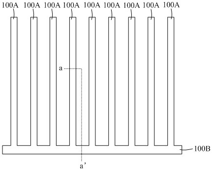
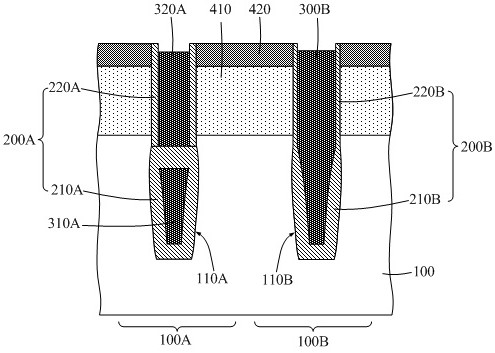
[0090] figure 2 is a layout structure of the semiconductor device in Embodiment 1 of the present invention, image 3 for figure 2 The schematic cross-sectional view of the semiconductor structure in the first embodiment of the present invention in the aa' direction is shown. Such as figure 2 with image 3 As shown, the semiconductor device includes a substrate 100 on which a cellular region 100A and a non-cellular region are defined. Wherein, shielded gate field effect transistors are formed in the cellular region 100A. In this embodiment, the semiconductor device has multiple cellular regions 100A, so that multiple shielded gate field effect transistors can be formed. And, a super barrier rectifier (SBR) is formed in the non-cellular region.

[0091] continue to refer figure 2 with image 3 As shown, the shielded gate field effect transistor includes: a first trench 110A formed in the substrate of the cell region 100A; a first dielectric layer 200A covering the bo...

Embodiment 2

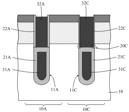
[0122] The difference from Embodiment 1 is that in this embodiment, the non-cellular region includes a rectification region and a source connection region, and the rectification region and the source connection region are respectively located in different regions to perform their corresponding functions. That is, a super-barrier rectifier is formed in the rectification region, and a source connection structure is formed in the source connection region.

[0123] Figure 4 It is the layout structure of the semiconductor device in the second embodiment of the present invention. Such as Figure 4 As shown, the non-cellular region includes a rectification region 100C and a source connection region 100B.

[0124] Wherein, the super-barrier rectifier is formed in the rectification region 100C. Specifically, the second trench of the super-barrier rectifier is formed in the substrate of the rectification region 100C, and the second dielectric layer and the second gate electrode are ...


PUM

PropertyMeasurementUnit
thicknessaaaaaaaaaa

Abstract

The invention provides a semiconductor device and a forming method thereof. According to the invention, a shielding gate field effect transistor is arranged in the cell region of the semiconductor device, a super-barrier rectifier is arranged in the non-cellular region, and the upper dielectric layer and the lower dielectric layer of the second dielectric layer in the super-barrier rectifier can be smoothly connected based on a beak structure, so that a tip structure between the upper dielectric layer and the lower dielectric layer of the second dielectric layer is avoided, and the problem that leakage current is easily caused due to the fact that the thickness of the bottom of the upper dielectric layer of the second dielectric layer is too thin can be effectively solved.

Description

technical field [0001] The invention relates to the technical field of semiconductors, in particular to a semiconductor device and a forming method thereof. Background technique [0002] A shielded gate field effect transistor (Shielded Gate Trench, SGT) is more conducive to the flexible application of semiconductor integrated circuits because of its low gate-to-drain capacitance Cgd, very low on-resistance, and high withstand voltage performance. Specifically, in the shielded gate field effect transistor, by setting the shielding electrode below the gate electrode, the gate-to-drain capacitance can be greatly reduced, and the drift region of the shielded gate field effect transistor also has a relatively high impurity carrier Concentration, can provide additional benefits to the breakdown voltage of the device, which can reduce the on-resistance accordingly. [0003] Furthermore, for semiconductor devices with shielded gate field effect transistors, in order to achieve fas...

Claims


Application Information

Patent Timeline
Patent Type & Authority Applications(China)
IPC IPC(8): H01L29/423H01L29/78H01L21/336
CPCH01L29/4236H01L29/7831H01L29/66484H01L29/7813H01L29/407H01L29/66734H01L29/42368H01L29/7803H01L27/0727H01L27/088H01L21/823487H01L21/823456H01L29/41H01L29/1095H01L29/41766
Inventor 宋金星丛茂杰袁家贵
Owner SEMICON MFG ELECTRONICS (SHAOXING) CORP
Why Eureka
Try Eureka