Method for manufacturing indium ball array of small-center-distance focal plane detector
A technology of focal plane detector and center distance, which is applied in semiconductor/solid-state device manufacturing, electric solid-state devices, semiconductor devices, etc., can solve the problems of small size, uneven indium column, etc., and achieve improved connectivity and high equipment compatibility , Improve the effect of tolerance ability
- Summary
- Abstract
- Description
- Claims
- Application Information
AI Technical Summary
Problems solved by technology
Method used
Image


Examples
Embodiment 1
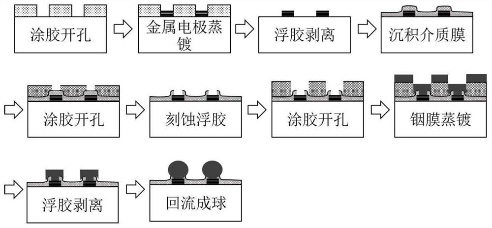
[0029]The purpose of this embodiment is to use the manufacturing method of the high-uniformity indium ball array disclosed in the present invention to produce a satisfying and readout circuit for an InAs / GaSb type II superlattice mid-wave infrared focal plane photosensitive chip with a center distance of 15 microns. The high-uniformity indium ball array required by flip-bonding verifies the feasibility of the present invention.
[0030] Based on the InAs / GaSb type II superlattice focal plane photosensitive chip after the p-contact electrode is prepared, the following steps are carried out:
[0031] (1) Using AZ4330 positive photoresist, through ultraviolet exposure and development, a square contact electrode hole pattern is produced in the center of the pixel. The sides of the holes are 7 microns long.
[0032] (2) Ion beam sputtering coating equipment is used to vapor-deposit three metal layers of chromium, nickel, and gold in sequence, with thicknesses of 100, 600, and 100 ...
Embodiment 2
[0043] The purpose of this embodiment is to produce an InGaAs / InAsP / InP short-wave infrared focal plane photosensitive chip with a center distance of 12.5 microns, using the manufacturing method of the high-uniformity indium ball array disclosed in the present invention, to produce a chip that meets the requirements of flip-bonding with the readout circuit. The high-uniformity indium ball array verifies the feasibility of the present invention.
[0044] Based on the nGaAs / InAsP / InP focal plane photosensitive chip after the p-contact electrode is prepared, the following steps are carried out:
[0045] (1) Using AZ4330 positive photoresist, through ultraviolet exposure and development, a square contact electrode hole pattern is produced in the center of the pixel. The sides of the holes are 6 microns long.
[0046] (2) Ion beam sputtering coating equipment is used to vapor-deposit three metal layers of chromium, nickel, and gold in sequence, with thicknesses of 50, 400, and 70 ...
Embodiment 3
[0057] The purpose of this embodiment is to use the manufacturing method of the high-uniformity indium ball array disclosed in the present invention for an InGaAs / InP short-wave infrared focal plane photosensitive chip with a center distance of 10 microns to produce a high-uniformity indium ball array that meets the requirements of flip-soldering with the readout circuit. permanent indium ball array to verify the feasibility of the present invention.
[0058] Based on the InGaAs / InP focal plane photosensitive chip after the p-contact electrode is prepared, the following steps are carried out:
[0059] (1) Using AZ4330 positive photoresist, through ultraviolet exposure and development, a square contact electrode hole pattern is produced in the center of the pixel. The side length of the hole is 5.5 microns.
[0060] (2) Ion beam sputtering coating equipment is used to vapor-deposit three metal layers of chromium, nickel, and gold in sequence, with thicknesses of 20, 200, and 5...
PUM
| Property | Measurement | Unit |
|---|---|---|
| Thickness | aaaaa | aaaaa |
| Thickness | aaaaa | aaaaa |
| Thickness | aaaaa | aaaaa |
Abstract
Description
Claims
Application Information
 - R&D
- Intellectual Property
- Life Sciences
- Materials
- Tech Scout
- Unparalleled Data Quality
- Higher Quality Content
- 60% Fewer Hallucinations
Browse by: Latest US Patents, China's latest patents, Technical Efficacy Thesaurus, Application Domain, Technology Topic, Popular Technical Reports.
© 2025 PatSnap. All rights reserved.Legal|Privacy policy|Modern Slavery Act Transparency Statement|Sitemap|About US| Contact US: help@patsnap.com