High-dielectric-constant gate dielectric material and preparation method thereof
A technology with high dielectric constant and gate dielectric, applied in nanotechnology, circuits, electrical components, etc. for materials and surface science, can solve problems such as poor interface quality, easy leakage, and poor reliability, and reduce the dielectric interface. The effect of increasing the density of states, improving the quality of the interface, and reducing the density of states at the interface
- Summary
- Abstract
- Description
- Claims
- Application Information
AI Technical Summary
Problems solved by technology
Method used
Image
Examples
Embodiment 1
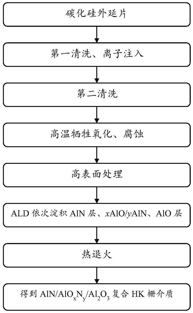
[0088] This embodiment provides a method for preparing a high dielectric constant gate dielectric material, the flow chart of which is shown in figure 1 , include,
[0089] (1) Pretreatment of silicon carbide epitaxial wafers
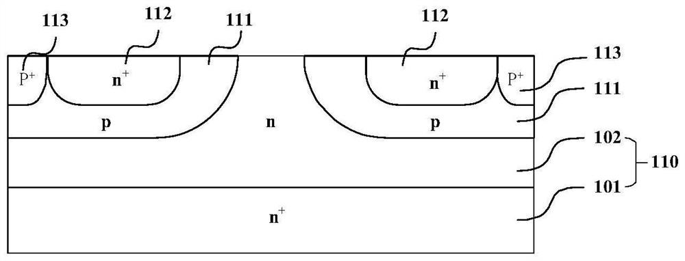
[0090] The silicon carbide epitaxial wafer 110 includes a substrate 101 and an epitaxial layer 102, such as figure 2 As shown, the substrate is (0001) n-type nitrogen-doped 4H-SiC with a 4 inclination angle, the thickness is 350 μm, and the resistivity is 0.001Ω·cm; the epitaxial layer is nitrogen-doped 6H-SiC, and the crystal orientation is the same as that of the substrate Same, the doping concentration is 1×10 15 cm -3 , with a thickness of 12 μm;
[0091] Perform the first cleaning on the epitaxial wafer, the first cleaning includes standard Piranha process cleaning, RCA process cleaning and DHF process cleaning; after cleaning, perform ion implantation process on the silicon carbide epitaxial wafer, so that the well region 111 and the base con...
Embodiment 2
[0099] This embodiment provides a method for preparing a high dielectric constant gate dielectric material, including:
[0100] (1) Pretreatment of silicon carbide epitaxial wafers
[0101] Such as Figure 8 As shown, a silicon carbide epitaxial wafer 210 includes a substrate 201, a first epitaxial layer 202, a second epitaxial layer 203, and a third epitaxial layer 204. The first epitaxial layer, the second epitaxial layer, and the third epitaxial layer are formed on the substrate crystal grow in the same crystal direction on the surface; wherein, the substrate 201 is (0001) n-type nitrogen-doped 4H-SiC with 4 tilt angles, the resistivity is 0.001Ω·cm, and the thickness is 350 μm; the first epitaxial layer 202 is n-type nitrogen-doped 4H-SiC with the same crystal orientation as the substrate, with a doping concentration of 5×10 15 cm -3 , with a thickness of 12 μm; the second epitaxial layer 203 is p-type aluminum-doped 4H-SiC with the same crystal orientation as the subst...
Embodiment 3
[0110] This embodiment provides a method for preparing a high dielectric constant gate dielectric material, including:
[0111] (1) Pretreatment of silicon carbide epitaxial wafers
[0112] The silicon carbide epitaxial wafer 310 includes a substrate 301 and an epitaxial layer 302, such as Figure 14 As shown, the substrate is semi-insulating undoped (0001) 4H-SiC with 4 dips, and the resistivity is greater than 10 5 Ω cm, the thickness is 350 μm, the epitaxial layer is n-type nitrogen-doped 4H-SiC, the crystal orientation is the same as that of the substrate, and the doping concentration is 5×10 15 cm -3 , the thickness of the epitaxial layer is 12 μm;
[0113] Perform the first cleaning on the epitaxial wafer 310, the first cleaning includes standard Piranha process cleaning, RCA process cleaning and DHF process cleaning; the cleaned silicon carbide epitaxial wafer is subjected to ion implantation process, so that the well region 311 and base contact are formed in the epi...
PUM
| Property | Measurement | Unit |
|---|---|---|
| Thickness | aaaaa | aaaaa |
| Thickness | aaaaa | aaaaa |
| Thickness | aaaaa | aaaaa |
Abstract
Description
Claims
Application Information
 - R&D
- Intellectual Property
- Life Sciences
- Materials
- Tech Scout
- Unparalleled Data Quality
- Higher Quality Content
- 60% Fewer Hallucinations
Browse by: Latest US Patents, China's latest patents, Technical Efficacy Thesaurus, Application Domain, Technology Topic, Popular Technical Reports.
© 2025 PatSnap. All rights reserved.Legal|Privacy policy|Modern Slavery Act Transparency Statement|Sitemap|About US| Contact US: help@patsnap.com


