LCP packaging substrate with built-in passive resistance-capacitance element and manufacturing method

A technology for packaging substrates and resistance-capacitance components, which is applied to electrical components, resistors, capacitors, etc., which can solve the problem of large influence of process material limitations, resistance and capacitance accuracy, and LCP surface quality. problems, to achieve the effect of improving circuit performance, increasing surface utilization, and reducing the difference in resistance or capacitance

Active Publication Date: 2020-08-07
SHANGHAI SPACEFLIGHT ELECTRONICS & COMM EQUIP RES INST
View PDF11 Cites 0 Cited by
  • Summary
  • Abstract
  • Description
  • Claims
  • Application Information

AI Technical Summary

Problems solved by technology

This method embeds resistors and capacitors with low accuracy and is greatly affected by the limitation of process materials
[0006] The second is to use sputtering or evaporation process to directly manufacture resistors and capacitors on the LCP substrate, but the surface of the LCP needs to be surface treated to improve adhesion. The accuracy of resistors and capacitors is greatly affected by the quality of the LCP surface

Method used


Image

  • LCP packaging substrate with built-in passive resistance-capacitance element and manufacturing method
  • LCP packaging substrate with built-in passive resistance-capacitance element and manufacturing method
  • LCP packaging substrate with built-in passive resistance-capacitance element and manufacturing method

Examples


Embodiment 1

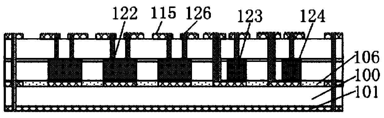
[0072] like figure 1 and Figures 4a to 4d As shown in , the present invention discloses an LCP package substrate with embedded passive resistance-capacitance elements, comprising:

[0073] Thin film resistance and capacitance, including thin film resistor 122 and thin film capacitor 123, two electrodes of the thin film resistor 122 are electroplated copper posts, and the upper electrode of the thin film capacitor 123 is electroplated copper posts;

[0074] The bottom plate of the LCP substrate includes a thin film RC embedded region 104 and a first LCP substrate positioning through hole 105;

[0075] At least one LCP substrate transition piece, including a first thin film resistor embedded frame 106, a first thin film capacitor embedded frame 107, a first thin film capacitor lower electrode lead-out through hole 108 and a second LCP substrate positioning through hole 109;

[0076] At least two LCP substrate bonding sheets, including a second thin film resistor embedded fram...

Embodiment 2

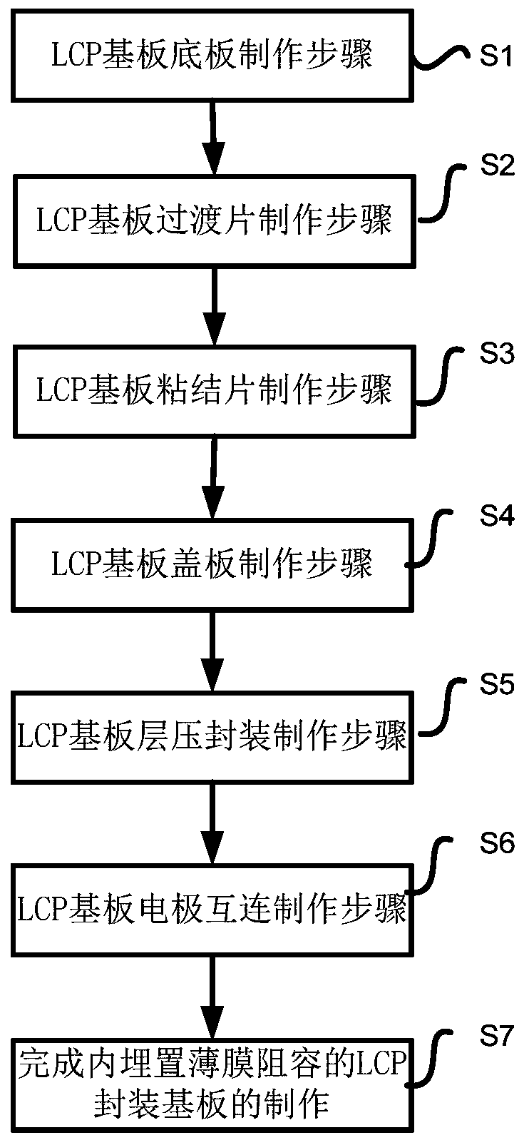
[0084] like figure 2 and 3a As shown in ~31, the present invention further discloses a method for manufacturing an LCP package substrate with embedded thin film resistance and capacitance, using the above-mentioned LCP package substrate with embedded thin film resistance and capacitance for manufacturing, including the following steps:

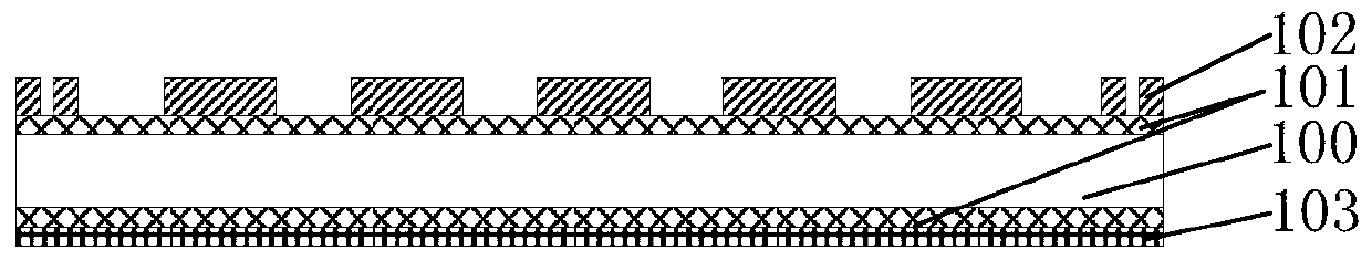
[0085] Step A: The LCP substrate bottom plate fabrication step, providing an LCP substrate 100 with a double-sided copper clad layer 101 , the back of the substrate is covered with a copper-clad tape 103 for protection, and the front of the substrate is subjected to photoresist 102 lithography, pattern electroplating Cu / Ni / Au, wet etching, forming a thin film resistance-capacitance buried area 104 on the front side of the substrate, removing the adhesive tape 103 on the back side, and then processing the first LCP substrate positioning through hole 105 by ultraviolet laser to form the LCP substrate bottom plate;

[0086] Step B: the LCP sub...


PUM

PropertyMeasurementUnit
thicknessaaaaaaaaaa
sizeaaaaaaaaaa
thicknessaaaaaaaaaa

Abstract

The invention discloses an LCP packaging substrate with a built-in passive resistance-capacitance element and a manufacturing method. The LCP packaging substrate comprises a thin film resistor-capacitor,an LCP substrate base plate, at least one LCP substrate transition sheet, at least two LCP substrate bonding sheets, and an LCP substrate cover plate, wherein theLCP substrate bottom plate, theLCPsubstrate bonding sheet, theLCP substrate transition sheet, thethin film resistor-capacitor, theLCP substrate bonding sheet and theLCP substrate cover plate are laminated and packaged twice in sequence, one LCP substrate bonding sheet is located between two LCP substrates, and electrodes of the thin film resistor-capacitor are led out through surface layer electrode electroplating copper columns.The high-precision and high-stability thin-film resistor and the thin-film capacitor are buried in the LCP packaging substrate in a multi-layer laminated packaging mode, the thin-film resistor-capacitors can be flexibly buried among multiple layers according to the size design, the surface utilization rate of the LCP substrate is greatly increased, and the substrate assembly density is improved.

Description

technical field [0001] The invention relates to the field of microelectronic packaging, in particular to an LCP packaging substrate with embedded passive resistance-capacitance elements and a manufacturing method. Background technique [0002] With the urgent requirements for small, lightweight, high-speed and multi-functional military electronic equipment and the rapid development of semiconductor integrated circuits, the scale of hybrid integrated circuits is getting larger and larger, especially for the research of electronic systems applied in the fields of radio frequency and microwave. It has become the focus of the electronic system industry, which puts forward higher requirements for lightweight, high-integration, and high-frequency packaging substrate materials. And with the increasing degree of integration of electronic systems, more and more functions are integrated into the packaging substrate, how to maximize the integration of passive components in the limited ...

Claims


Application Information

Patent Timeline
Patent Type & Authority Applications(China)
IPC IPC(8): H01L49/02H01L23/522
CPCH01L23/5223H01L23/5228H01L28/20H01L28/40
Inventor 丁蕾刘凯罗燕张诚陈桂莲王立春
Owner SHANGHAI SPACEFLIGHT ELECTRONICS & COMM EQUIP RES INST
Why Eureka
Try Eureka