Solar blind ultraviolet light detector based on amorphous (GaLu)2O3 film
A detector and ultraviolet light technology, applied in the direction of semiconductor devices, sustainable manufacturing/processing, electrical components, etc., can solve the problems of crystal quality degradation, degradation of device electrical performance and stability, etc., to reduce dark current and improve detection capabilities , the effect of speeding up the response speed
- Summary
- Abstract
- Description
- Claims
- Application Information
AI Technical Summary
Problems solved by technology
Method used
Image
Examples
Embodiment 1
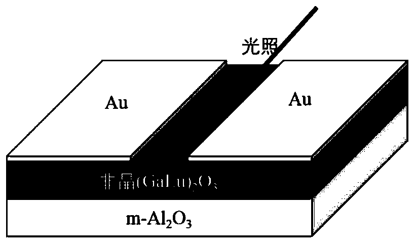
[0049] Such as figure 1 As shown, the present embodiment is based on an amorphous (GaLu) 2 o 3 Thin-film sun-blind ultraviolet light detector, the detector includes an m-plane sapphire substrate, an active layer, and a pair of parallel metal electrodes from bottom to top, wherein: the active layer is amorphous (GaLu) 2 o 3 film, the material of the parallel metal electrodes is Au. The thickness of the substrate is 0.43 mm, the thickness of the active layer is 120 nm, the thickness of the parallel metal electrodes is 50 nm, and the distance between the parallel metal electrodes is 10 μm.
[0050] In this embodiment, the above-mentioned amorphous (GaLu) based 2 o 3 The thin-film sun-blind ultraviolet light detector is prepared by the following method, including the following steps:
[0051] Step 1: Preparation by solid phase sintering (GaLu) 2 o 3 Ternary ceramic target
[0052] 1.1 molar ratio Ga 2 o 3 : Lu 2 o 3 =95:5, weigh 8.995g Ga 2 o 3 powder and 1.005g Lu ...
Embodiment 2
[0060] Embodiment 2 (comparative example)
[0061] A single crystal (GaLu) based 2 o 3 Thin-film sun-blind ultraviolet photodetector, the detector includes c-plane sapphire substrate, active layer, and a pair of parallel metal electrodes from bottom to top, wherein: the active layer is (GaLu) 2 o 3 thin film, the material of the parallel metal electrodes is Au, the thickness of the substrate is 0.43 mm, the thickness of the active layer is 150 nm, the thickness of the parallel metal electrodes is 55 nm, and the distance between the parallel metal electrodes is 10 μm .
[0062] In this embodiment, the above-mentioned single crystal (GaLu) based 2 o 3 The thin-film sun-blind ultraviolet light detector is prepared by the following method, including the following steps:
[0063] Step 1: (GaLu) prepared by the same solid phase sintering method as in Example 1 2 o 3 Ternary ceramic target
[0064] Step 2 utilizes (GaLu) 2 o 3 Preparation of solar-blind ultraviolet light d...
Embodiment 3
[0069] Embodiment 3 (comparative example)
[0070] A β-Ga based 2 o 3 Thin-film sun-blind ultraviolet light detector, the detector includes a c-plane sapphire substrate, an active layer, and a pair of parallel metal electrodes from bottom to top, wherein: the active layer is β-Ga 2 o 3 thin film, the material of the parallel metal electrodes is Au, the thickness of the substrate is 0.43 mm, the thickness of the active layer is 150 nm, the thickness of the parallel metal electrodes is 55 nm, and the distance between the parallel metal electrodes is 10 μm .
[0071] The above-mentioned β-Ga-based 2 o 3 The thin-film sun-blind ultraviolet light detector is prepared by the following method, including the following steps:
[0072] Step 1: Preparation of Ga by sintering by solid phase sintering method 2 o 3 Ceramic target
[0073] 1.1 Weigh 10g Ga 2 o 3 Powder, add 15g of deionized water, then place in the ball mill jar (the ball milling medium is zirconia ceramic balls) ...
PUM
| Property | Measurement | Unit |
|---|---|---|
| Thickness | aaaaa | aaaaa |
| Thickness | aaaaa | aaaaa |
| Thickness | aaaaa | aaaaa |
Abstract
Description
Claims
Application Information
 - Generate Ideas
- Intellectual Property
- Life Sciences
- Materials
- Tech Scout
- Unparalleled Data Quality
- Higher Quality Content
- 60% Fewer Hallucinations
Browse by: Latest US Patents, China's latest patents, Technical Efficacy Thesaurus, Application Domain, Technology Topic, Popular Technical Reports.
© 2025 PatSnap. All rights reserved.Legal|Privacy policy|Modern Slavery Act Transparency Statement|Sitemap|About US| Contact US: help@patsnap.com


