Perovskite battery and preparation method thereof
A perovskite cell, perovskite technology, applied in the field of solar cells, can solve the problems of large optics, thin film optics, narrow band gap, loss, etc.
- Summary
- Abstract
- Description
- Claims
- Application Information
AI Technical Summary
Problems solved by technology
Method used
Image
Examples
Embodiment 1
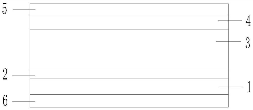
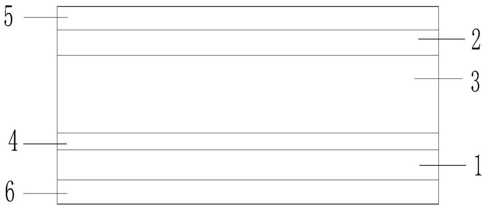
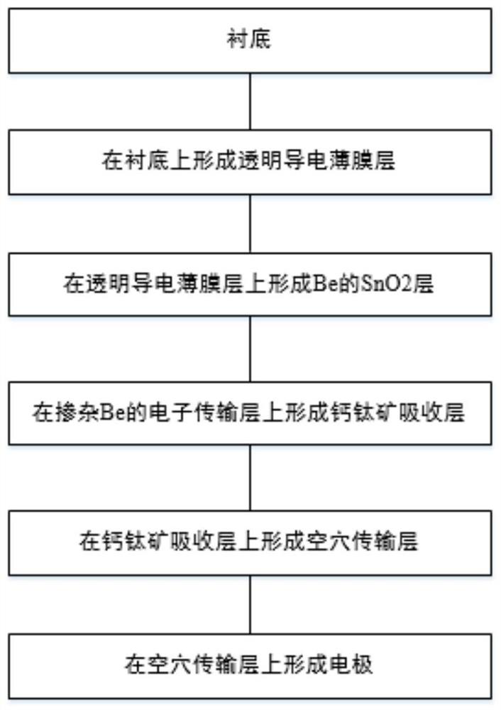
[0065] Select glass substrate as the substrate;
[0066] Depositing an ITO transparent conductive film layer with a thickness of 200nm on the substrate;
[0067] Deposit Be-containing SnO with a thickness of 50nm on the ITO transparent conductive film layer 2 thin film layer, where SnO 2 : Be molar ratio is 1:0.05;
[0068] In Be-containing SnO 2 Spin-coat FAPbI with a thickness of 500 nm on the thin film layer 3 film layer;
[0069] In FAPbI 3 The Spiro-OMeTAD film layer with a thickness of 100nm is spin-coated on the film layer;
[0070] On the Spiro-OMeTAD thin film layer, gold with a thickness of 80nm was vapor-deposited as an electrode.
Embodiment 2
[0072] Select glass substrate as the substrate;
[0073] Depositing an ITO transparent conductive film layer with a thickness of 200nm on the substrate;
[0074] Deposit Be-containing SnO with a thickness of 50nm on the ITO transparent conductive film layer 2 thin film layer, where SnO 2 : Be molar ratio is 1:0.09;
[0075] In Be-containing SnO 2 Spin-coat FAPbI with a thickness of 500 nm on the thin film layer 3 film layer;
[0076] In FAPbI 3 The Spiro-OMeTAD film layer with a thickness of 100nm is spin-coated on the film layer;
[0077] On the Spiro-OMeTAD thin film layer, gold with a thickness of 80nm was vapor-deposited as an electrode.
Embodiment 3
[0079] Select glass substrate as the substrate;
[0080] Depositing an ITO transparent conductive film layer with a thickness of 200nm on the substrate;
[0081] Deposit Be-containing SnO with a thickness of 50nm on the ITO transparent conductive film layer 2 thin film layer, where SnO 2 : Be molar ratio is 1:0.01;
[0082] In Be-containing SnO 2 Spin-coat FAPbI with a thickness of 500 nm on the thin film layer 3 film layer;
[0083] In FAPbI 3 The Spiro-OMeTAD film layer with a thickness of 100nm is spin-coated on the film layer;
[0084] On the Spiro-OMeTAD thin film layer, gold with a thickness of 80nm was vapor-deposited as an electrode.
[0085] For the perovskite cell that comparative example, embodiment 1, embodiment 2 and embodiment 3 make are tested, adopt the steady-state light source IV tester to measure the current density of battery (mA / cm 2 ), voltage (V), fill factor and Eff (photoelectric conversion efficiency) to obtain the test results shown in Table ...
PUM
| Property | Measurement | Unit |
|---|---|---|
| Thickness | aaaaa | aaaaa |
| Thickness | aaaaa | aaaaa |
| Thickness | aaaaa | aaaaa |
Abstract
Description
Claims
Application Information
 - Generate Ideas
- Intellectual Property
- Life Sciences
- Materials
- Tech Scout
- Unparalleled Data Quality
- Higher Quality Content
- 60% Fewer Hallucinations
Browse by: Latest US Patents, China's latest patents, Technical Efficacy Thesaurus, Application Domain, Technology Topic, Popular Technical Reports.
© 2025 PatSnap. All rights reserved.Legal|Privacy policy|Modern Slavery Act Transparency Statement|Sitemap|About US| Contact US: help@patsnap.com


