
Annealing method of oxide semiconductor film by utilizing deep ultraviolet laser

An oxide semiconductor and deep ultraviolet technology, which is applied in semiconductor/solid-state device manufacturing, electrical components, circuits, etc., can solve the problems of inability to meet large-scale and low-temperature processing, long annealing time, easy to damage the substrate, etc., and the time to reach is short. , the treatment range can be selected, the effect of low energy consumption

Inactive Publication Date: 2019-05-17
SOUTH CHINA UNIV OF TECH
View PDF4 Cites 1 Cited by
  • Summary
  • Abstract
  • Description
  • Claims
  • Application Information

AI Technical Summary

Problems solved by technology

These traditional annealing methods have problems such as high power consumption, long annealing time, and easy damage to the substrate.
[0004] Therefore, the traditional high-temperature thermal annealing can no longer meet the large-size and low-temperature processing (<350°C) requirements of today's flexible display devices.

Method used


Image

  • Annealing method of oxide semiconductor film by utilizing deep ultraviolet laser
  • Annealing method of oxide semiconductor film by utilizing deep ultraviolet laser
  • Annealing method of oxide semiconductor film by utilizing deep ultraviolet laser

Examples


Embodiment 1

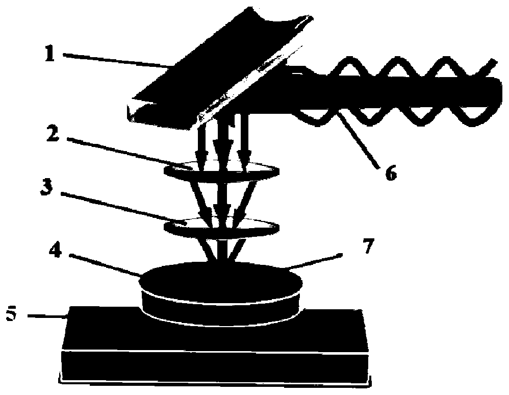
[0030] A method for annealing an oxide semiconductor thin film using a deep ultraviolet laser, comprising the following steps:

[0031] First, prepare an amorphous oxide semiconductor thin film on a clean glass substrate with a vacuum magnetron sputtering apparatus;

[0032] Next, treat the film with a deep ultraviolet laser: (1) Set the beam moving speed to 1230mm / s; (2) Set the energy density and power of the laser according to the thickness of the film sample, and then set the horizontal overlap and vertical spacing of the beam movement ; (3) Place the film flat on the sample stage, set the minimum distance between the laser lens and the sample to be 101 μm, and scan the light beam horizontally and continuously on the film sample according to the above parameters until all areas are affected.


PUM

PropertyMeasurementUnit
Vertical spacingaaaaaaaaaa
Thicknessaaaaaaaaaa

Abstract

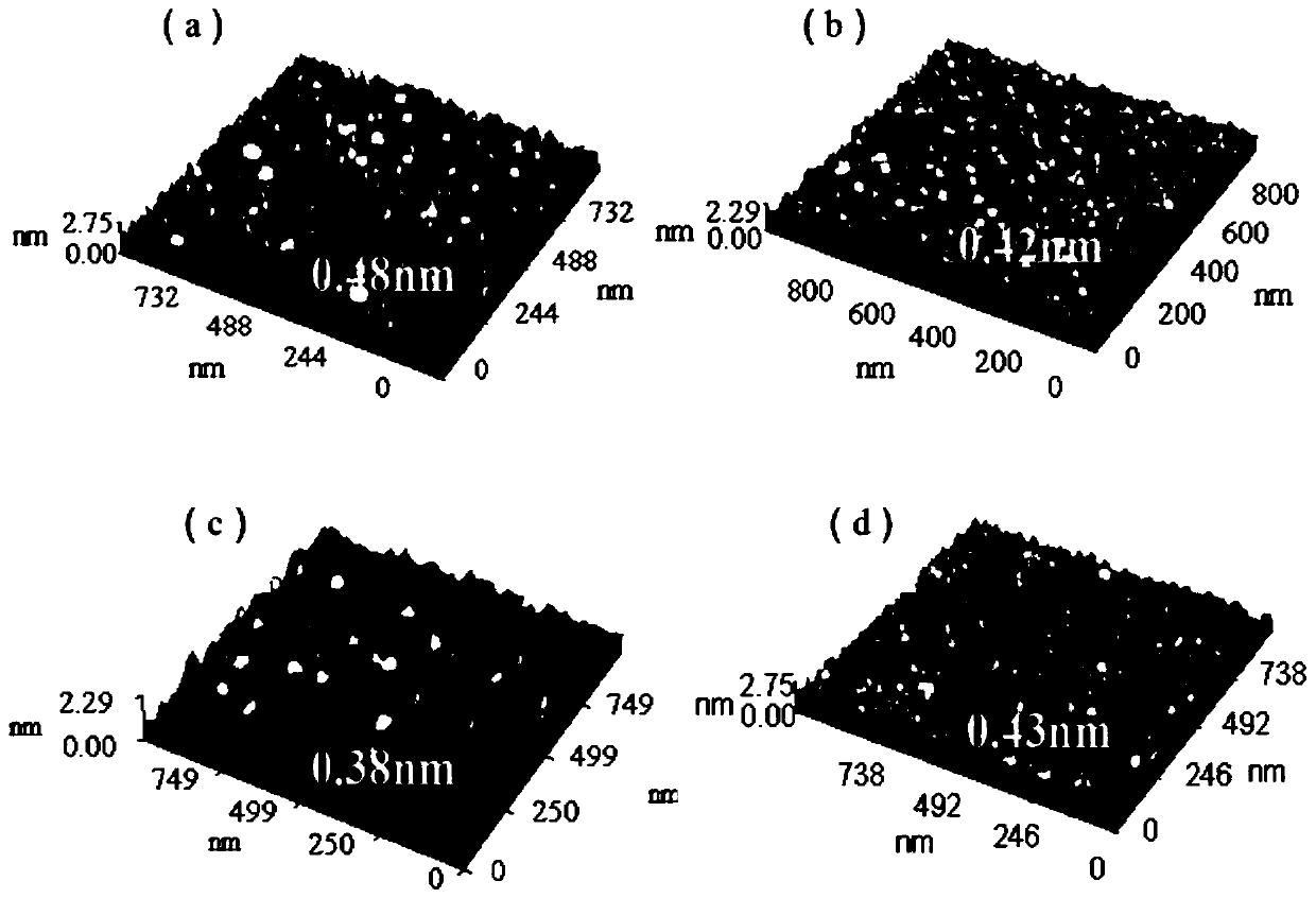
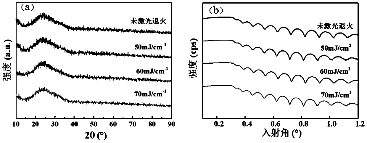
The invention belongs to the field of deep ultraviolet laser annealing, and discloses an annealing method of an oxide semiconductor film by utilizing deep ultraviolet laser. The method comprises the following steps of preparing an amorphous oxide semiconductor film on a glass substrate, horizontally placing the film on a sample stage, setting a minimum distance between a laser device lens and a film sample, setting a movement speed of a laser beam, setting a transverse overlapping rate and a longitudinal spacing of beam movement, and then performing transverse continuous scanning by the laserbeam till all areas are effected. According to the method, continuous scanning is performed on the film by the deep ultraviolet laser, so that the surface topography, the physical property and the optical characteristic of the film are improved; the luminous transmittance is improved; and an optical band gap of STO by laser treatment is increased. Compared with the traditional high-temperature heat treatment, the method has the advantages of high energy, optional treatment range, short time, low energy consumption and the like; and the time for effecting a complete 10*10mm sample is only 1.98s.

Description

technical field [0001] The invention belongs to the field of deep ultraviolet laser annealing, in particular to a method for annealing an oxide semiconductor thin film by using a deep ultraviolet laser. Background technique [0002] The performance of the amorphous STO thin film prepared by magnetron sputtering is generally poor, and it needs to be annealed to improve the performance of the thin film. [0003] Currently common annealing techniques are (1) vacuum annealing method; (2) heat pipe test annealing furnace method; (3) contact type high current annealing furnace method; (4) induction annealing furnace method. These traditional annealing methods all have problems such as high power consumption, long annealing time, and easy damage to the substrate. [0004] Therefore, the traditional high-temperature thermal annealing can no longer meet the large-size and low-temperature processing (<350°C) requirements of today's flexible display devices. Since Soviet scholars ...

Claims


Application Information

Patent Timeline
IPC IPC(8): H01L21/02H01L21/428H01L21/477
Inventor 宁洪龙邓宇熹姚日晖刘贤哲袁炜健张啸尘张观广张旭梁志豪彭俊彪
Owner SOUTH CHINA UNIV OF TECH
Learn More