


Quick Research
Generate reliable direction feasibility study reports for your R&D in just a few steps.

Technical Q&A
Discover and master advanced knowledge NOW. Basics, ideas, possibilities, all at once.

Find Solutions
As an expert in R&D theories, this can generate solutions to your technical problems instantly.

Evaluate Feasibility
Analyze your overall solution with one click, know your potential R&D risks in advance.

Monitor Landscape
Get weekly tech updates, stay abreast of the latest tech innovations and key insights.
Photoelectric programming polymorphic memory based on thin film transistor structure and manufacturing method thereof
A thin-film transistor and memory technology, applied in the field of multi-state memory and its preparation, to achieve low power consumption requirements, good film uniformity, and high storage density
- Summary
- Abstract
- Description
- Claims
- Application Information
AI Technical Summary
Problems solved by technology
Method used
Image

Examples
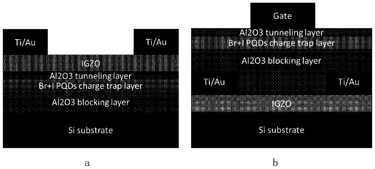
Embodiment 1
[0040] Embodiment 1 Bottom gate structure
[0041] Step 1, put the conductive substrate into the atomic layer deposition reaction chamber, the temperature range of the deposition chamber is 20°C-40°C, the temperature range of the TMA source bottle and each pipeline is 20°C-40°C, and vacuumize;
[0042] In step 2, an aluminum oxide barrier layer is prepared by atomic layer deposition. With trimethylaluminum and oxygen plasma as the reaction source, each cycle includes: 0.1s-2s trimethylaluminum pulse, 10s-30s nitrogen purge, 0.1s-10s oxygen plasma pulse, 10s-30s nitrogen purge sweep. Thickness range 30nm-50nm;
[0043] Step 3, with PbBr2, CsBr, PbI2, CsI, dimethylformamide, oleic acid, oleylamine, anhydrous toluene, methyl acetate, normal hexane etc., solution method prepares CsPbBr3, CsPbI3 perovskite quantum dot, and with Spin coating evenly on the barrier layer at a specific speed;
[0044] In step 4, an aluminum oxide tunneling layer is prepared by a low-temperature ato...
Embodiment 2
[0048] Example 2 Top Gate Structure
[0049] Step 1, put the substrate into the magnetron sputtering to grow the IGZO channel layer, define the channel pattern by ultraviolet lithography, and etch with dilute hydrochloric acid;
[0050] Step 2, define the pattern of the source and drain electrodes by photolithography again, remove the glue with acetone, and evaporate the Ti / Au source and drain electrodes by electron beam. Thickness range 70nm-130nm;
[0051] Step 3, put it into the atomic layer deposition reaction chamber, the temperature range of the deposition chamber is 20°C-40°C, the temperature range of the TMA source bottle and each pipeline is 20°C-40°C, and vacuumize;
[0052] In step 4, an aluminum oxide barrier layer is prepared by atomic layer deposition. With trimethylaluminum and oxygen plasma as the reaction source, each cycle includes: 0.1s-2s trimethylaluminum pulse, 10s-30s nitrogen purge, 0.1s-10s oxygen plasma pulse, 10s-30s nitrogen purge sweep. Thickne...
PUM
| Property | Measurement | Unit |
|---|---|---|
| thickness | aaaaa | aaaaa |
| thickness | aaaaa | aaaaa |
| thickness | aaaaa | aaaaa |
Abstract
Description
Claims
Application Information
 - R&D Engineer
- R&D Manager
- IP Professional
- Industry Leading Data Capabilities
- Powerful AI technology
- Patent DNA Extraction
Browse by: Latest US Patents, China's latest patents, Technical Efficacy Thesaurus, Application Domain, Technology Topic, Popular Technical Reports.
© 2024 PatSnap. All rights reserved.Legal|Privacy policy|Modern Slavery Act Transparency Statement|Sitemap|About US| Contact US: help@patsnap.com