Diamond field effect transistor based on Al2O3/SiNx double-layer gate medium and preparation method of diamond field effect transistor
A field-effect transistor and diamond technology, applied in transistors, semiconductor/solid-state device manufacturing, semiconductor devices, etc., can solve the problems of poor dielectric quality, limiting the characteristics and stability of diamond electronic devices, and low gate electrode withstand voltage of devices. The effect of large output current, improved concentration and stability, and high saturation output current
- Summary
- Abstract
- Description
- Claims
- Application Information
AI Technical Summary
Problems solved by technology
Method used
Image


Examples
Embodiment 1
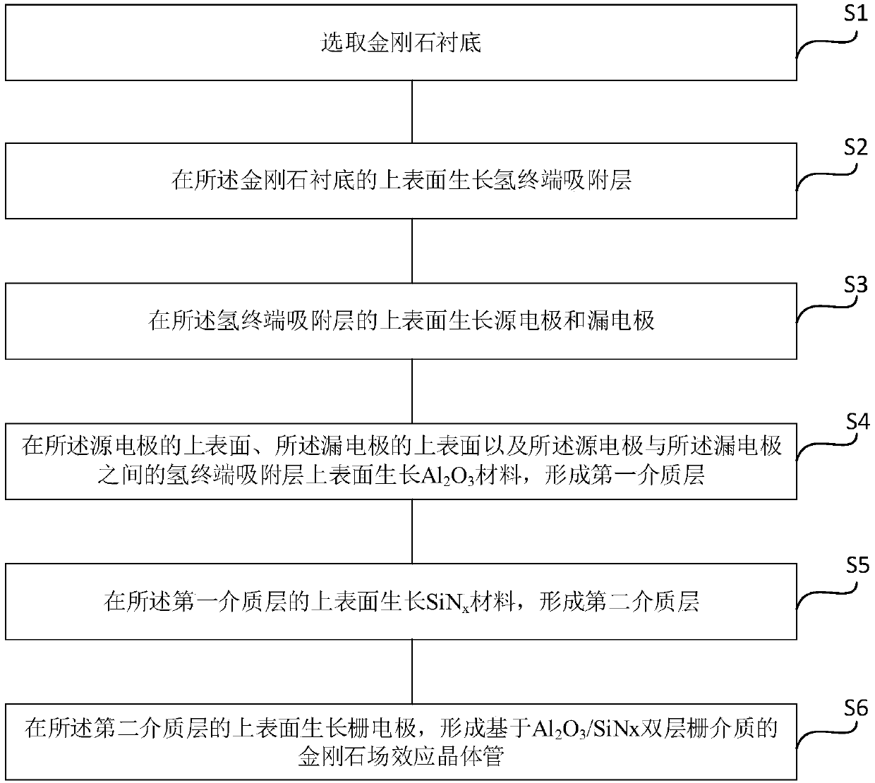
[0054] See figure 1 , figure 1 It is an Al-based 2 o 3 / SiN x Flowchart of the method for preparing a diamond field effect transistor with a double-layer gate dielectric. The preparation method of the present embodiment comprises:
[0055] S1: select the diamond substrate;
[0056] S2: growing a hydrogen terminal adsorption layer on the upper surface of the diamond substrate;
[0057] S3: growing a source electrode and a drain electrode on the upper surface of the hydrogen terminal adsorption layer;
[0058] S4: growing Al on the upper surface of the source electrode, the upper surface of the drain electrode, and the upper surface of the hydrogen terminal adsorption layer between the source electrode and the drain electrode 2 o 3 material, forming the first dielectric layer;
[0059] S5: growing SiN on the upper surface of the first dielectric layer x material, forming the second dielectric layer;
[0060] S6: grow a gate electrode on the upper surface of the second...
Embodiment 2
[0084] On the basis of the above-mentioned embodiments, the present embodiment takes the substrate as single crystal diamond, Al 2 o 3 / SiN x Taking a diamond field effect transistor with a double-layer gate dielectric thickness of 30 nm as an example, the preparation method of the embodiment of the present invention will be described in detail. See Figure 2a-Figure 2f as well as image 3 and Figure 4 , Figure 2a-Figure 2f It is an Al-based 2 o 3 / SiN x Schematic diagram of the preparation process of a diamond field effect transistor with a double-layer gate dielectric, image 3 is a schematic structural diagram of a first mask provided by an embodiment of the present invention; Figure 4 is a schematic structural diagram of a second mask provided by an embodiment of the present invention.
[0085] The preparation method of the present embodiment comprises:
[0086] Step 1: Select a single crystal diamond substrate 1 .
[0087] A single crystal diamond with a th...
Embodiment 3
[0104] On the basis of the above-mentioned embodiments, the present embodiment takes the substrate as polycrystalline diamond, Al 2 o 3 / SiN x Taking a diamond field effect transistor with a total thickness of a double-layer gate dielectric of 50 nm as an example, the preparation method of the embodiment of the present invention will be described in detail.
[0105] refer again Figure 2a to Figure 2f , the preparation method of the present embodiment comprises:
[0106] Step 1: Select a polycrystalline diamond substrate 1 .
[0107] Polycrystalline diamond with a thickness of 1 mm was selected as the substrate.
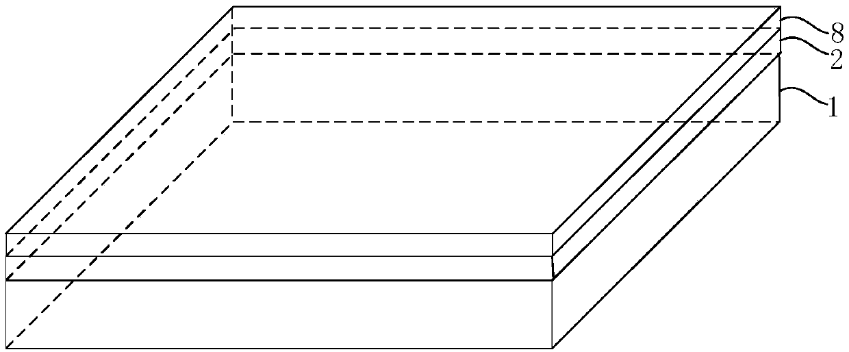
[0108] Step 2: forming a hydrogen terminal adsorption layer 2 on the upper surface of the diamond substrate 1 .
[0109] Specifically, the single crystal diamond 1 substrate is placed in the reaction chamber of MPCVD, and hydrogen gas with a flow rate of 800 sccm is introduced to form a hydrogen plasma; the pressure in the reaction chamber is 800 mbar, the react...
PUM
| Property | Measurement | Unit |
|---|---|---|
| thickness | aaaaa | aaaaa |
| thickness | aaaaa | aaaaa |
| thickness | aaaaa | aaaaa |
Abstract
Description
Claims
Application Information
 - R&D
- Intellectual Property
- Life Sciences
- Materials
- Tech Scout
- Unparalleled Data Quality
- Higher Quality Content
- 60% Fewer Hallucinations
Browse by: Latest US Patents, China's latest patents, Technical Efficacy Thesaurus, Application Domain, Technology Topic, Popular Technical Reports.
© 2025 PatSnap. All rights reserved.Legal|Privacy policy|Modern Slavery Act Transparency Statement|Sitemap|About US| Contact US: help@patsnap.com