A ret IGBT with self-biased pmos and its fabrication method
A self-biasing, split gate technology, applied in semiconductor/solid-state device manufacturing, semiconductor devices, electrical components, etc., can solve problems such as reducing device switching speed, increasing device switching loss, and device breakdown voltage degradation.
- Summary
- Abstract
- Description
- Claims
- Application Information
AI Technical Summary
Problems solved by technology
Method used
Image

Examples
Embodiment 1
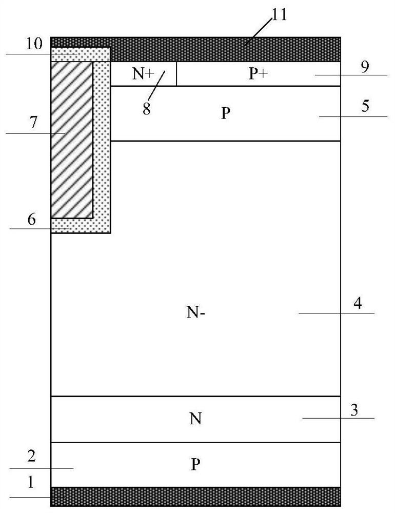
[0051] An embodiment of a RET IGBT device with self-biased PMOS, as figure 2 As shown, it includes: back collector metal 1, P-type collector region 2, N-type field stop layer 3 and N-drift region 4 stacked sequentially from bottom to top, with a trench gate structure above the N-drift region 4 , the trench structure includes a gate dielectric layer 6, a gate electrode 7, and a dielectric layer 10 above the gate dielectric layer 6 and the gate electrode 7; it is characterized in that: a P-type buried layer 12 is placed above the N-drift region 4, A split gate structure, the split gate structure includes a polycrystalline split gate electrode 15, a gate dielectric layer 14; the upper part of the P-type buried layer 12 has an N-type charge storage layer 13; the upper part of the N-type charge storage layer 13 has a P-type base region 5; the upper part of the P-type base region 5 has an N+ emitter region 8 and a P+ contact region 9; 11; the gate electrode 7 is connected to the N-...
Embodiment 2
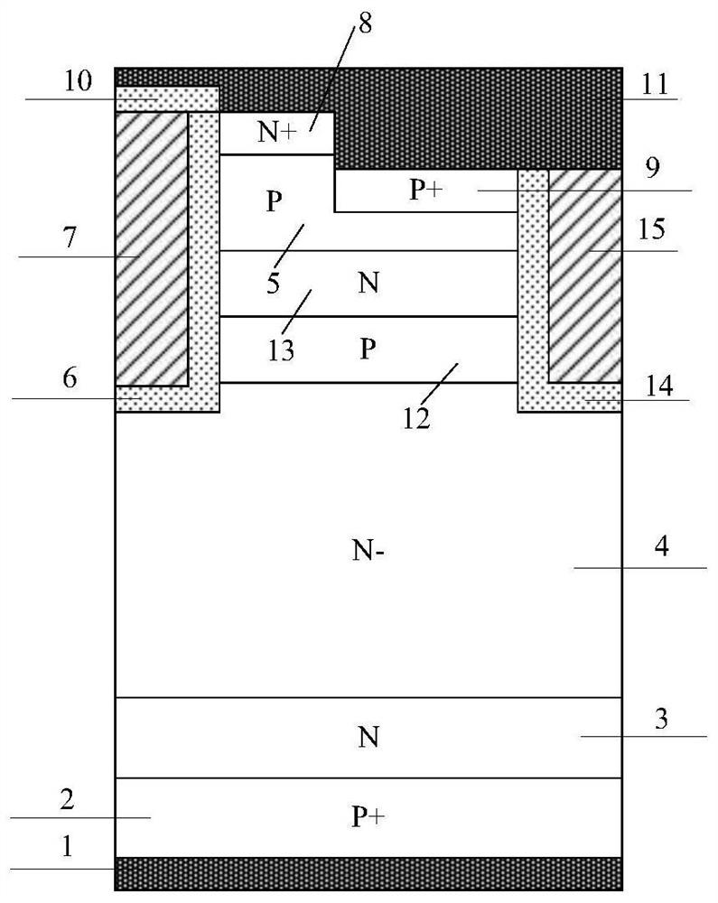
[0053] An embodiment of a RET IGBT device with self-biased PMOS, as image 3 As shown, it includes: back collector metal 1, P-type collector region 2, N-type field stop layer 3 and N-drift region 4 stacked sequentially from bottom to top, with a trench gate structure above the N-drift region 4 , the trench structure includes a gate dielectric layer 6, a gate electrode 7, a dielectric layer 10 above the gate dielectric layer 6 and the gate electrode 7; it is characterized in that there is a P-type buried layer 12 above the N-drift region 4, separating Gate structure, the separated gate structure includes a polycrystalline separated gate electrode 15, a gate dielectric layer 14; the upper part of the P-type buried layer 12 has an N-type charge storage layer 13; the upper part of the N-type charge storage layer 13 has a P-type base region 5; the upper part of the P-type base region 5 has an N+ emitter region 8 and a P+ contact region 9; The upper part of 9 has a Schottky contact...
Embodiment 3
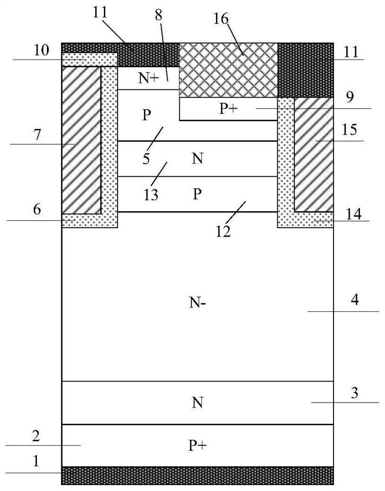
[0055] An embodiment of a RET IGBT device with self-biased PMOS, as Figure 4 As shown, on the basis of Example 1, a super junction structure composed of super junction N pillars 41 and super junction P pillars 42 is introduced into the drift region, and the junction depth of the super junction P pillars 42 is less than or equal to the junction depth of the super junction N pillars 41. deep, a separate gate electrode 71 is introduced below the gate electrode 71 , and the separate gate electrode 71 is short-circuited with the separate gate electrode 15 .
[0056] The introduction of the super junction structure further reduces the turn-on voltage drop of the device and increases the breakdown voltage of the device, and the introduction of the separated gate electrode 71 further reduces the Miller capacitance of the device.
PUM
 Abstract
Description
Claims
Application Information
 - R&D
- Intellectual Property
- Life Sciences
- Materials
- Tech Scout
- Unparalleled Data Quality
- Higher Quality Content
- 60% Fewer Hallucinations
Browse by: Latest US Patents, China's latest patents, Technical Efficacy Thesaurus, Application Domain, Technology Topic, Popular Technical Reports.
© 2025 PatSnap. All rights reserved.Legal|Privacy policy|Modern Slavery Act Transparency Statement|Sitemap|About US| Contact US: help@patsnap.com