A UV detector with a double-doped Al composition graded separation layer
An ultraviolet detector and a technology of composition gradient, applied in the field of ultraviolet detectors, can solve the problems of reducing the ionization energy of electron holes, enhancing the piezoelectric polarization effect, affecting the crystal quality of the device, etc., so as to enhance the polarization electric field, reduce the Lattice mismatch, the effect of increasing the avalanche multiplication factor
- Summary
- Abstract
- Description
- Claims
- Application Information
AI Technical Summary
Problems solved by technology
Method used
Image
Examples
Embodiment 1
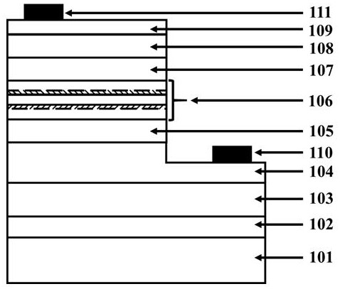
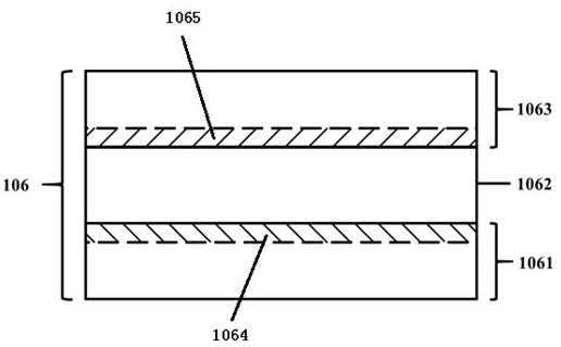
[0022] An ultraviolet detector with a double-doped Al composition graded separation layer, including a substrate 101, an AlN intermediate layer 102, a non-doped i-Al x1 Ga 1-x1 N buffer layer 103, n-type n-Al x2 Ga 1-x2 N layer 104, non-doped i-Al x3 Ga 1-x3 N absorption layer 105, double-doped Al composition graded p-Al x4 Ga 1-x4 N / i-Al x5 Ga 1-x5 N / n-Al x6 Ga 1-x6 N separation layer 106, non-doped i-Al x7 Ga 1-x7 N multiplication layer 107, p-type p-Al x8 Ga 1-x8 N layer 108 and p-type GaN layer 109; in n-type n-Al x1 Ga 1-x1 An n-type ohmic electrode 110 is drawn out on the N layer 104, and a p-type ohmic electrode 111 is drawn out on the p-type GaN layer 109, wherein x1, x2, x3, x4, x5, x6, x7, x8 satisfy x1>x2=x3=x4> x5>x6=x7>x8.
[0023] Such as figure 1 Shown is the ultraviolet detector provided by the present invention with double-doped Al composition gradient separation layer, c-plane sapphire substrate 101, AlN intermediate layer 102, non-doped i-Al...
Embodiment 2
[0032] An ultraviolet detector with a double-doped Al composition graded separation layer, including a substrate 101, an AlN intermediate layer 102, a non-doped i-Al x1 Ga 1-x1 N buffer layer 103, n-type n-Al x2 Ga 1-x2 N layer 104, non-doped i-Al x3 Ga 1-x3 N absorption layer 105, double-doped Al composition graded p-Al x4 Ga 1-x4 N / i-Al x5 Ga 1-x5 N / n-Al x6 Ga 1-x6 N separation layer 106, non-doped i-Al x7 Ga 1-x7 N multiplication layer 107, p-type p-Al x8 Ga 1-x8 N layer 108 and p-type GaN layer 109; in n-type n-Al x1 Ga 1-x1 An n-type ohmic electrode 110 is drawn out on the N layer 104, and a p-type ohmic electrode 111 is drawn out on the p-type GaN layer 109, wherein x1, x2, x3, x4, x5, x6, x7, x8 satisfy x1>x2=x3=x4> x5>x6=x7>x8.
[0033] Such as figure 1 Shown is the ultraviolet detector provided by the present invention with double-doped Al composition gradient separation layer, c-plane sapphire substrate 101, AlN intermediate layer 102, non-doped i-Al...
Embodiment 3
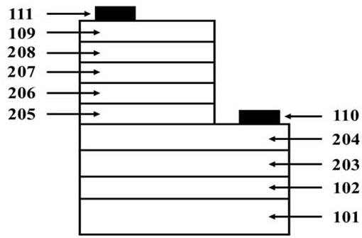
[0042] An ultraviolet detector with a double-doped Al composition graded separation layer, including a substrate 101, an AlN intermediate layer 102, a non-doped i-Al x1 Ga 1-x1 N buffer layer 103, n-type n-Al x2 Ga 1-x2 N layer 104, non-doped i-Al x3 Ga 1-x3 N absorption layer 105, double-doped Al composition graded p-Al x4 Ga 1-x4 N / i-Al x5 Ga 1-x5 N / n-Al x6 Ga 1-x6 N separation layer 106, non-doped i-Al x7 Ga 1-x7 N multiplication layer 107, p-type p-Al x8 Ga 1-x8 N layer 108 and p-type GaN layer 109; in n-type n-Al x1 Ga 1-x1 An n-type ohmic electrode 110 is drawn out on the N layer 104, and a p-type ohmic electrode 111 is drawn out on the p-type GaN layer 109, wherein x1, x2, x3, x4, x5, x6, x7, x8 satisfy x1>x2=x3=x4> x5>x6=x7>x8.
[0043] Such as figure 1 Shown is the ultraviolet detector provided by the present invention with double-doped Al composition gradient separation layer, c-plane sapphire substrate 101, AlN intermediate layer 102, non-doped i-Al...
PUM
| Property | Measurement | Unit |
|---|---|---|
| thickness | aaaaa | aaaaa |
| thickness | aaaaa | aaaaa |
| thickness | aaaaa | aaaaa |
Abstract
Description
Claims
Application Information
 - R&D Engineer
- R&D Manager
- IP Professional
- Industry Leading Data Capabilities
- Powerful AI technology
- Patent DNA Extraction
Browse by: Latest US Patents, China's latest patents, Technical Efficacy Thesaurus, Application Domain, Technology Topic, Popular Technical Reports.
© 2024 PatSnap. All rights reserved.Legal|Privacy policy|Modern Slavery Act Transparency Statement|Sitemap|About US| Contact US: help@patsnap.com


