
Method for preparing magnetic tunnel junction array

A technology of magnetic tunnel junctions and arrays, applied in the fields of magnetic field-controlled resistors, electromagnetic device manufacturing/processing, electrical components, etc., can solve problems such as memory layer short circuit, low etching rate, and radiation damage, and achieve Conducive to miniaturization, elimination of redeposition, and improvement of electrical properties

Active Publication Date: 2019-06-25
SHANGHAI CIYU INFORMATION TECH
View PDF4 Cites 1 Cited by
  • Summary
  • Abstract
  • Description
  • Claims
  • Application Information

AI Technical Summary

Problems solved by technology

The re-deposition of magnetic tunnel junction material or chemical etching by-products due to physical sputtering will cover the sidewall of the magnetic tunnel junction after etching. Usually, after the etching process is completed, a layer will be formed on the sidewall The damaged layer / deposited layer, for the RIE process, will also bring about radiation damage (Irradiation Damage), which will affect the magnetic and electrical properties of the magnetic tunnel junction, and what's more, it will directly cause damage from the reference layer. Short circuit to the memory layer, which is not conducive to the improvement of the yield of magnetic memory
At the same time, the etching rate of the RIE or IBE process is not very high, which is very unfavorable for its mass production.

Method used


Image

  • Method for preparing magnetic tunnel junction array
  • Method for preparing magnetic tunnel junction array
  • Method for preparing magnetic tunnel junction array

Examples


Embodiment Construction

[0028] In order to make the above objects, features and advantages of the present invention more comprehensible, specific implementations of the present invention will be described in detail below in conjunction with the accompanying drawings. It should be noted that all the drawings of the present invention are in simplified form and use inaccurate scales, and are only used to facilitate and clearly assist the purpose of illustrating the embodiments of the present invention.

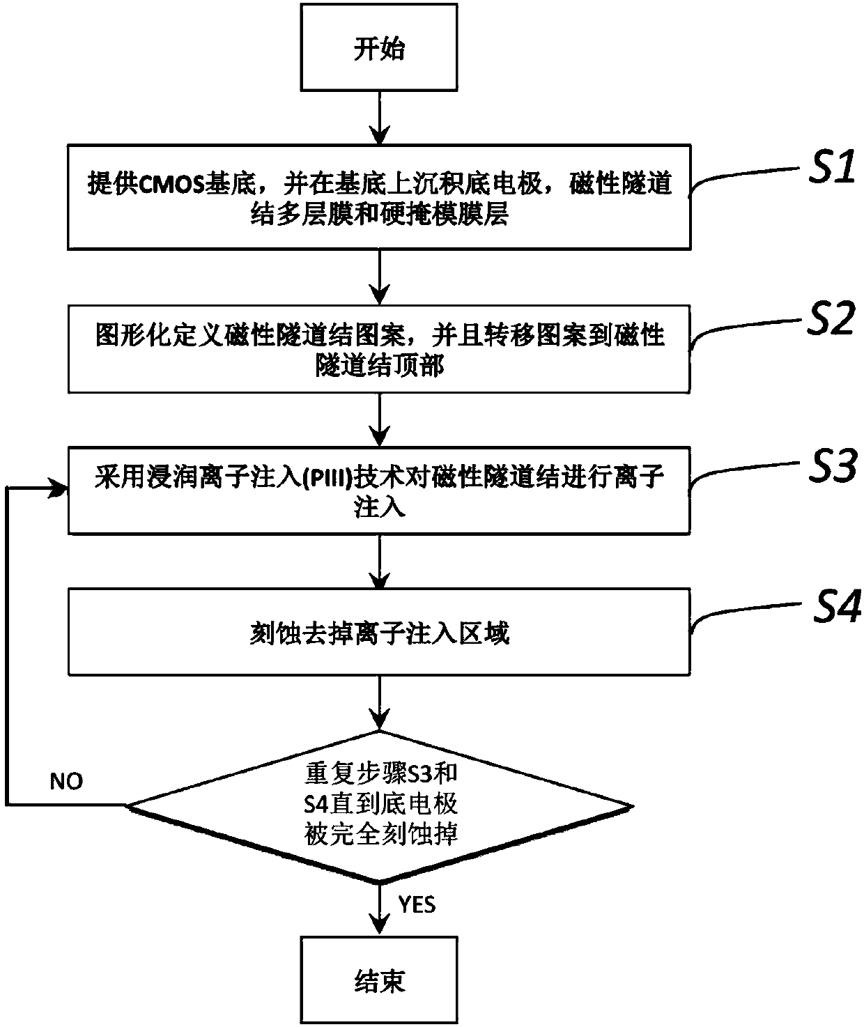
[0029] The present invention provides a method for preparing a magnetic tunnel junction array using a combined process flow of immersion ion implantation and etching. The material is modified so that it can generate volatile by-products in the subsequent etching process, and then the modified magnetic tunnel junction thin layer is removed by reactive ion etching (RIE, Reactive Ion Etching); repeated wetting ion implantation ( PIII) and reactive ion etching (RIE) process until the bottom electrode layer ...


PUM


Abstract

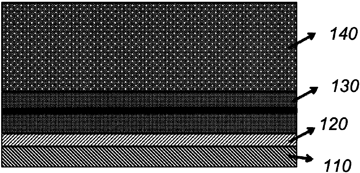
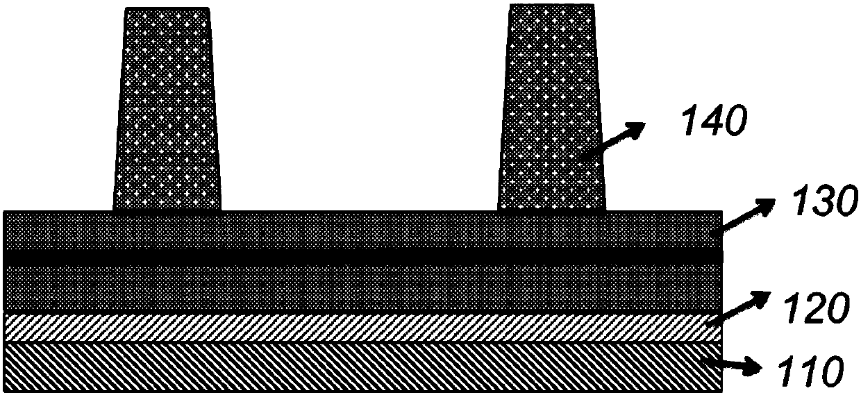
The invention provides a method for preparing a magnetic tunnel junction array, which includes the following steps: S1, providing a CMOS substrate, and depositing a bottom electrode layer, a magnetictunnel junction multilayer film and a hard mask layer on the substrate; S2, graphically defining a magnetic tunnel junction pattern and transferring the pattern to the top of the magnetic tunnel junction multilayer film; S3, implanting ions into the edges of the magnetic tunnel junction multilayer film and the hard mask layer; S4, removing the ion implantation area of the magnetic tunnel junctionmultilayer film by etching; and S5, repeating S3 and S4 until the etching of the magnetic tunnel junction multilayer film and the bottom electrode layer is completed. The beneficial effect of the method is as follows: because the etching byproduct can easily form volatile gas which is exhausted from an exhaust device in the etching process, the re-deposition of the etching byproduct will be eliminated, which is conducive to the improvement of magnetic and electrical properties and yield of magnetic random access memories and the miniaturization of magnetic random access memories.

Description

technical field [0001] The invention relates to a method for preparing a magnetic tunnel junction array, in particular to a process flow combining immersion ion implantation (PIII, Plasma Immersion Ion Implantation) and etching to prepare a magnetic tunnel junction (MTJ, Magnetic Tunnel Junction) array The method belongs to the magnetic random access memory (MRAM, Magnetic Radom Access Memory) manufacturing technology field. Background technique [0002] In recent years, MRAM using magnetic tunnel junction (MTJ) has been considered as the future solid-state non-volatile memory, which has the characteristics of high-speed reading and writing, large capacity and low energy consumption. Ferromagnetic MTJ is usually a sandwich structure, which has a magnetic memory layer, which can change the magnetization direction to record different data; an insulating tunnel barrier layer in the middle; a magnetic reference layer, located on the other side of the tunnel barrier layer, which ...

Claims


Application Information

Patent Timeline
IPC IPC(8): H01L43/08H01L43/12H01L27/22
Inventor 张云森
Owner SHANGHAI CIYU INFORMATION TECH
Learn More