Diamond/graphene composite heat conduction film, preparation method thereof and heat dissipation system
A graphene composite, diamond thin film technology, applied in chemical instruments and methods, heat exchange materials, metal material coating processes, etc., can solve the problems of low binding force between graphene and diamond, complex preparation process, and high interface thermal resistance. , to achieve the effect of easy industrial production and use, excellent thermal conductivity structure, and excellent heat dissipation performance
- Summary
- Abstract
- Description
- Claims
- Application Information
AI Technical Summary
Problems solved by technology
Method used
Image
Examples
preparation example Construction
[0041] The second aspect of the embodiment of the present invention provides a method for preparing a diamond / graphene composite heat-conducting film, including:
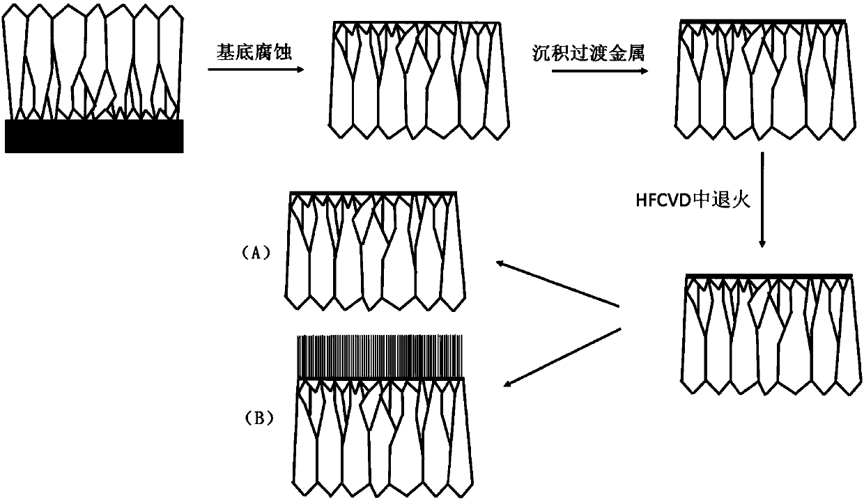
[0042] S01, providing a substrate, depositing a microcrystalline diamond film on the surface of the substrate;
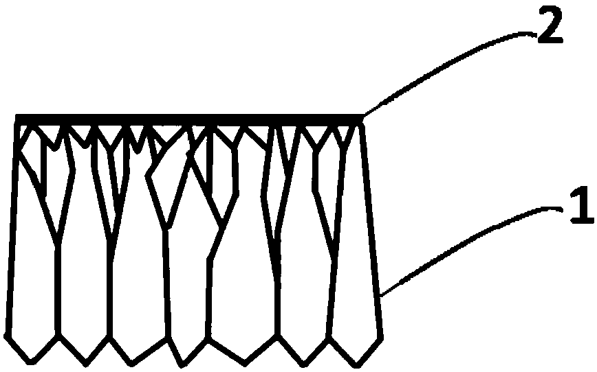
[0043] S02, removing the substrate by etching to obtain a self-supporting microcrystalline diamond film; wherein, the self-supporting microcrystalline diamond film includes a surface to be nucleated, and the surface to be nucleated is the microcrystalline diamond film before etching a contact surface with said substrate;
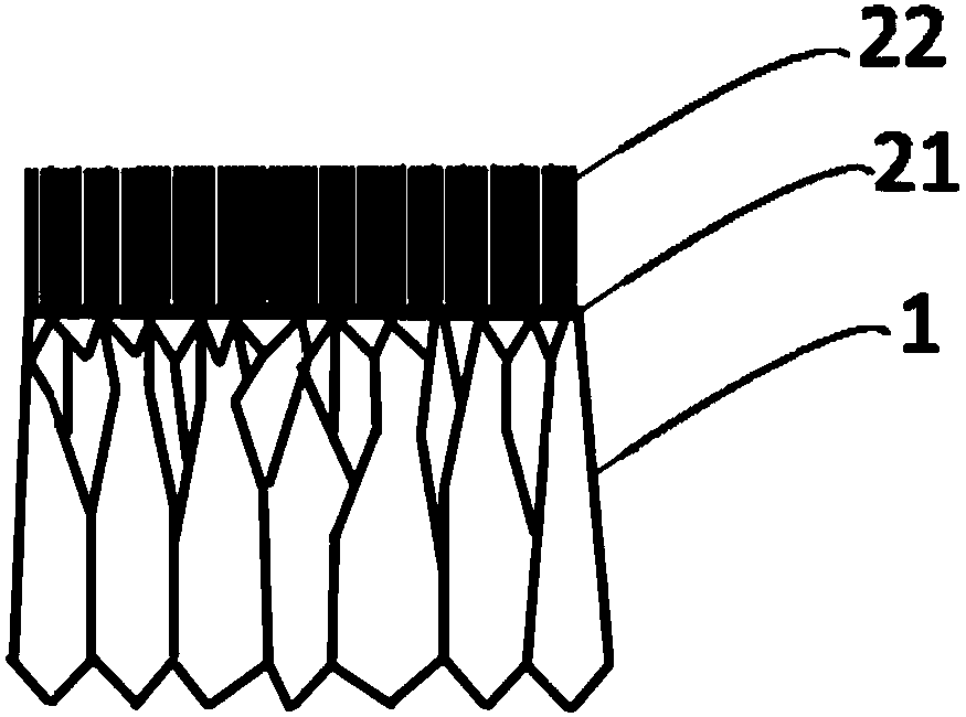
[0044] S03, depositing a transition metal layer on the surface to be nucleated, placing the self-supporting microcrystalline diamond film deposited with the transition metal layer in the cavity of a hot wire vapor deposition chamber for rapid annealing, the transition metal layer The transition metal catalyzes part of the carbon elements in the microcrystalline diamond film to form a g...
Embodiment 1
[0079] A kind of diamond / graphene composite heat conduction film and preparation method thereof, it comprises the steps:
[0080] (1) Depositing a highly thermally conductive microcrystalline diamond film on the surface of a silicon substrate:
[0081] Microcrystalline diamond thin film preparation method 1: a 1 mm thick diamond thin film layer is prepared on a single crystal (100) silicon wafer with a size of Φ200 mm by using the hot wire chemical vapor deposition (HFCVD) method. Place silicon wafers in NH before growth 4 OH / H 2 o 2 / deionized water (1:1:5) mixed solution, heated to 70 ° C for 1 hour, rinsed the silicon wafer, then put the silicon wafer in acetone solution for ultrasonic cleaning for 10 minutes, and deionized water for 10 minutes , ultrasonic cleaning in alcohol solution for 10 minutes. Subsequently, the cleaned silicon wafer was placed in the suspension of nano-diamond powder for ultrasonic treatment for 1 hour. The average particle size of the diamond...
Embodiment 2
[0087] A kind of diamond / graphene composite heat conduction film and preparation method thereof, it comprises the steps:
[0088] Step (1) is with embodiment 1;
[0089] (2) Preparation of graphene layer on the surface of microcrystalline diamond film:
[0090] (a) Put the diamond / silicon sample into a mixed solution of hydrofluoric acid / sulfuric acid / glacial acetic acid at a ratio of 1:1:2 to corrode the silicon substrate (or put it into a 30% (w / v) KOH solution, heat to 85°C for silicon etching), and the etching time is 5-24 hours. Then the obtained self-supporting diamond film was washed and dried. The smooth diamond surface obtained after etching the silicon substrate is called the diamond film nucleation surface. Using the bottom surface of diamond as the deposition surface of high-purity nickel metal, put the self-supporting diamond film into the electron beam deposition equipment, turn on the equipment until the background vacuum reaches 10 -8 Torr, turn on the elec...
PUM
| Property | Measurement | Unit |
|---|---|---|
| Thickness | aaaaa | aaaaa |
| Diameter | aaaaa | aaaaa |
Abstract
Description
Claims
Application Information
 - R&D
- Intellectual Property
- Life Sciences
- Materials
- Tech Scout
- Unparalleled Data Quality
- Higher Quality Content
- 60% Fewer Hallucinations
Browse by: Latest US Patents, China's latest patents, Technical Efficacy Thesaurus, Application Domain, Technology Topic, Popular Technical Reports.
© 2025 PatSnap. All rights reserved.Legal|Privacy policy|Modern Slavery Act Transparency Statement|Sitemap|About US| Contact US: help@patsnap.com


