
Super-junction device and manufacturing method thereof

A technology of superjunction device and manufacturing method, applied in semiconductor/solid state device manufacturing, semiconductor devices, electrical components, etc., can solve problems such as threshold voltage exceeding specifications

Active Publication Date: 2018-08-21
SHENZHEN SANRISE TECH CO LTD
View PDF4 Cites 1 Cited by
  • Summary
  • Abstract
  • Description
  • Claims
  • Application Information

AI Technical Summary

Problems solved by technology

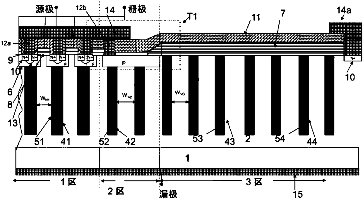
[0016] For devices formed through the above process, the dose of JFET implantation, that is, the N-type ion implantation in the JFET region corresponding to lithography 2, is about an order of magnitude smaller than that of Pwell, that is, the implantation of P-type wells, and the impact is very small. Therefore, the device’s The threshold voltage is basically determined by the Pwell implant dose, so that the implant under the P-type guard ring is the same as the Pwell implant without adding an additional P-type guard ring lithography and implantation, and the P-type guard ring is located in the transition region. , so usually the P-type protection ring and Pwell are formed at the same time, and it is also represented by Pwell. In the case of a general threshold voltage of 2-4 volts, the Pwell implant dose is generally 3E13cm -2 ~5E13cm -2 , while the JFET injection dose is at 1E12cm -2 ~3E12cm -2 , too high a Pwell injection dose will cause the threshold voltage to exceed the specification

Method used


Image

  • Super-junction device and manufacturing method thereof
  • Super-junction device and manufacturing method thereof
  • Super-junction device and manufacturing method thereof

Examples


Embodiment Construction

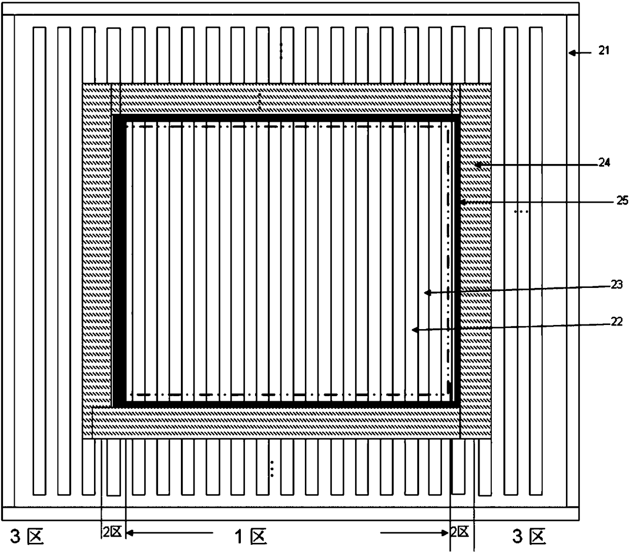
[0072] like figure 1 As shown, it is a top view of an existing superjunction device; a general superjunction device structure includes a charge flow region, a terminal region laterally subjected to a reverse bias voltage, and a transition region between the charge flow region and the terminal region, and the terminal region around the periphery of the charge flow region, figure 1 Zone 1 represents the charge flow region, Zone 2 represents the transition region, and Zone 3 represents the terminal region.

[0073] Zone 1 includes a super junction structure composed of alternately arranged P-type pillars 22 and N-type pillars 23, figure 1 Both the P-type pillars 22 and the N-type pillars 23 are strip-shaped. The N-type pillar 23 provides a conduction path when the super-junction device is turned on, and the P-type pillar 22 and the N-type pillar 23 deplete each other and bear the reverse bias together when the super-junction device is reverse-biased.

[0074] Region 2 and Regi...


PUM


Abstract

The invention discloses a super-junction device, which is characterized in that a protective epoxy film exposes a charge flow region, completely covers a transition region and completely or mostly covers a terminal region, the setting of the protective epoxy film enables a JFET region and a source region to realize comprehensive injection, and the JFET region is enabled to be overlapped with eachP-type well and reduces the doping concentration on the surface of each corresponding P-type well, thereby enabling the overall doping concentration of the P-type wells to be increased under the condition of maintaining the threshold voltage of the device to be unchanged, and being capable of improving the avalanche current tolerance of the device. The invention further discloses a manufacturing method of the super-junction device. The super-junction device can keep the threshold voltage of the device to be unchanged while improving the injection dose of the P-type wells, so that the charge flow region and the transition region are enabled to be improved in avalanche current tolerance, and thus the performance of the device is improved; and the number of times of the photoetching process can also be reduced, the performance and reliability of the device can be maintained, the manufacturing cost can be reduced, and the production cycle can be shortened.

Description

technical field [0001] The invention relates to a method for manufacturing a semiconductor integrated circuit, in particular to a method for manufacturing a superjunction device. Background technique [0002] The super junction structure is composed of alternately arranged N-type pillars and P-type pillars. If the superjunction structure is used to replace the N-type drift region in the vertical double-diffused MOS transistor (Vertical Double-diffused Metal-Oxide-Semiconductor, VDMOS) device, the conduction path is provided through the N-type column in the conduction state, and when the conduction The P-type column does not provide a conduction path; in the off state, the PN column jointly bears the reverse bias voltage, forming a super-junction metal-oxide-semiconductor field-effect transistor (Metal-Oxide-Semiconductor Field-Effect Transistor, MOSFET). The super-junction MOSFET can greatly reduce the on-resistance of the device by using a low-resistivity epitaxial layer w...

Claims


Application Information

Patent Timeline
IPC IPC(8): H01L29/06H01L29/78H01L21/336
CPCH01L29/0611H01L29/0615H01L29/0684H01L29/66477H01L29/78
Inventor 肖胜安曾大杰
Owner SHENZHEN SANRISE TECH CO LTD
Learn More