Method of fabricating image sensor and reworking method thereof

a technology of image sensor and reworking method, which is applied in the manufacture of semiconductor/solid-state devices, semiconductor devices, electrical devices, etc., can solve the problems of low product yield, high product cost, and inability to completely remove the capping layer 130/b>, and achieve the effect of reducing the photo lithography process, enhancing product yield, and relatively simple fabrication process

Active Publication Date: 2011-09-01
UNITED MICROELECTRONICS CORP
View PDF10 Cites 7 Cited by
  • Summary
  • Abstract
  • Description
  • Claims
  • Application Information

AI Technical Summary

Benefits of technology

[0026]In the method of present invention, until the color filter, the microlenses and the capping layer are formed in sequence, the etching step is performed to exposing the patterned metal layer above the pad region. In comparison to the conventional art, the method of the present invention can reduce a photo lithography process, thereby making the fabrication process relatively simple. Furthermore, there are not problems of incompletely removing the capping layer and over etching, so that the image sensor fabricated by the above method of present invention can be reworked. In addition, the method of reworking the image sensor of the present invention may avoid the problem that the whole image sensor should be rejected when observing the defects of the image sensor. Therefore, the product yield can be enhanced and the product cost can be reduced.

Problems solved by technology

However, the capping layer 130 can not be removed completely and easily.
Consequently, some problems, such as, rejecting the whole CMOS image sensor, low product yield and high product cost, would be generated.

Method used


Image

  • Method of fabricating image sensor and reworking method thereof
  • Method of fabricating image sensor and reworking method thereof
  • Method of fabricating image sensor and reworking method thereof

Examples


Embodiment Construction

[0031]FIGS. 2A to 2F are schematic, side cross-sectional view of an image sensor according to an embodiment of the present invention, when the image sensor is fabricated.

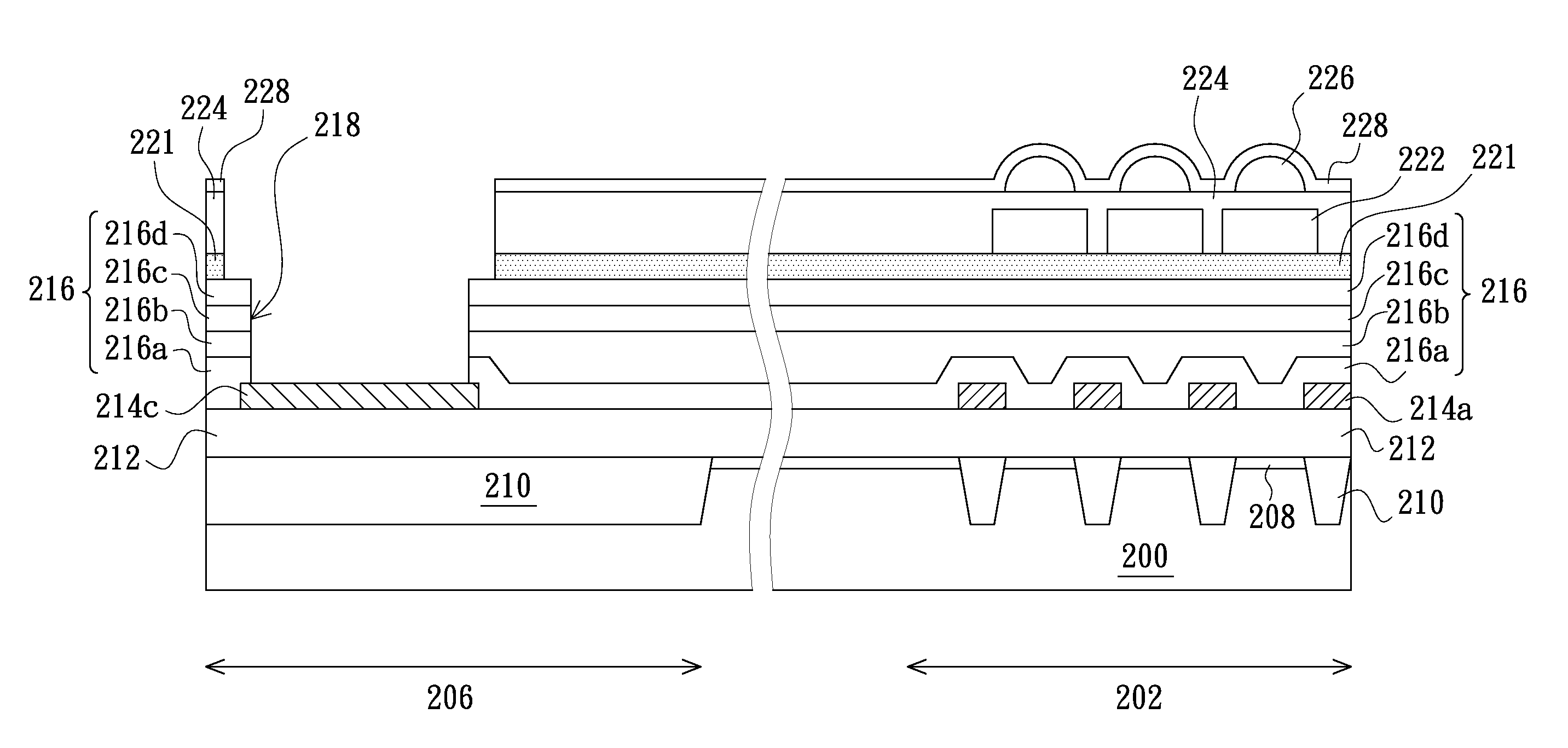
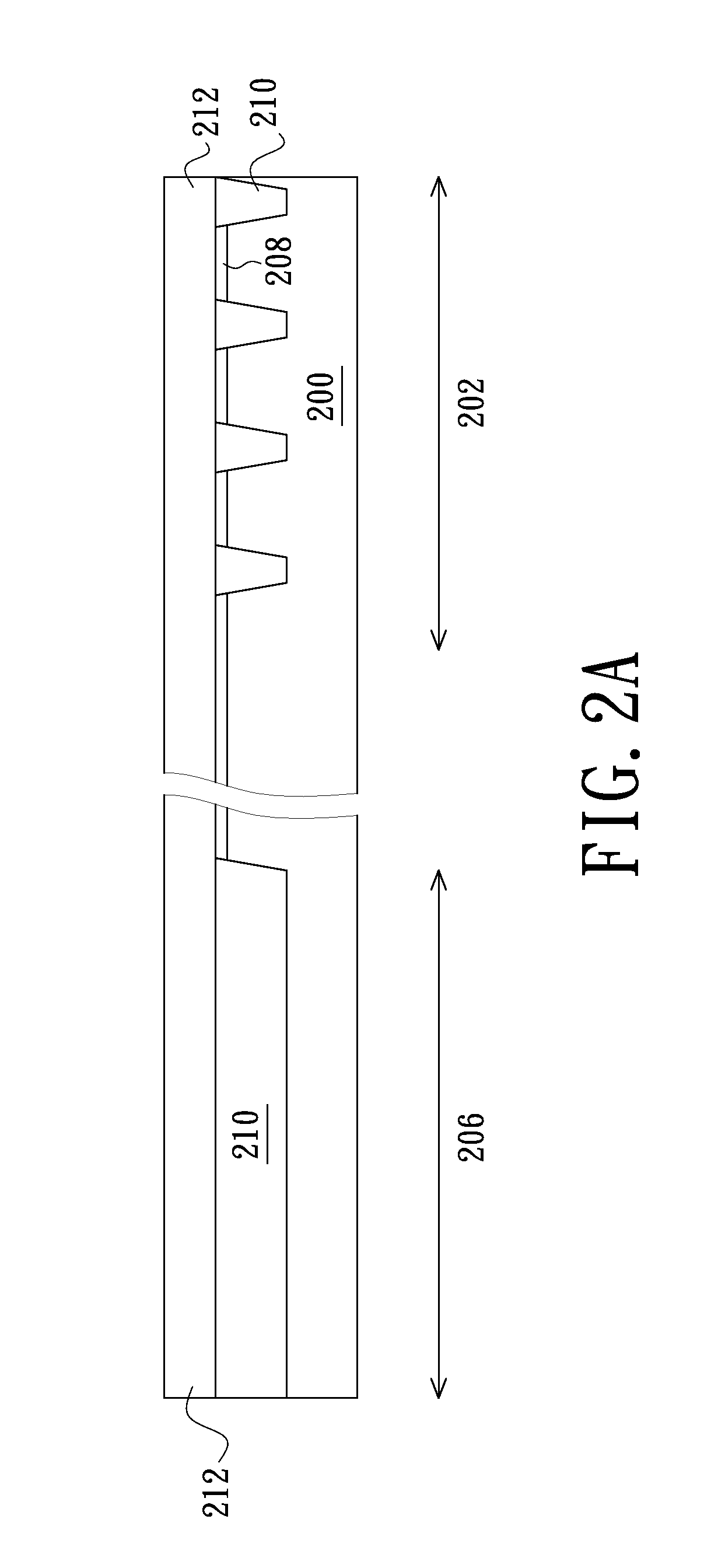
[0032]Firstly, referring to FIG. 2A, a substrate 200 is provided. The substrate 200 can be a semiconductor substrate. The substrate 200 having a pixel array region 202 and a pad region 206. A photo sensing unit array and a plurality of isolation structures 210 are formed the substrate 200. The photo sensing unit array is made of a plurality of photo sensing units 208. The isolation structures 210 are used to isolate the photo sensing units 208. The isolation structures 210 can be shallow trench isolation structures.

[0033]Next, a metal interconnect structure and a plurality of inter-layer dielectric layers 212 is formed on the substrate 200 to cover the photo sensing units 208. The metal interconnect structure and a plurality of inter-layer dielectric layers 212 can be made by a metal etching process, a dielectric de...


PUM


Abstract

A method of fabricating an image sensor device is provided. First, a substrate comprising a pixel array region and a pad region is provided. A patterned metal layer and a first planarization layer having an opening exposing the patterned metal layer in the pad region are sequentially formed on the substrate. A color filter array is formed on the first planarization layer in the pixel array region. A second planarization layer is formed to cover the color filter array and filled into the opening. A plurality of microlens is formed above the color filter array on the second planarization layer. A capping layer is conformally formed on the microlens and the second planarization layer. An etching step is performed to remove the capping layer and the second planarization layer in the opening so as to expose the patterned metal layer in the pad region.

Description

BACKGROUND[0001]1. Technical Field[0002]The present invention relates to a method of fabricating a semiconductor device, and more particularly to a method of fabricating an image sensor and a method of reworking an image sensor.[0003]2. Description of the Related Art[0004]Generally, optoelectronic devices that may convert light into electronic signals include CMOS image sensors (CISs) and charge coupled devices (CCDs).[0005]Because the CMOS image sensors can be used in a low voltage condition and fabricated by a CMOS process, production cost and size of the CMOS image sensors can be reduced dramatically. And thus, the CMOS image sensors have replaced the charge coupled devices to be used in digital electronics gradually.[0006]FIG. 1 is a schematic, side cross-sectional view of a conventional CMOS image sensor.[0007]Please referring to FIG. 1, the CMOS image sensor includes a substrate 100 having a pixel array region 101 and a pad region 103. A plurality of shallow trench isolation s...

Claims


Application Information

Patent Timeline
Patent Type & Authority Applications(United States)
IPC IPC(8): H01L31/0232H01L31/18H01L27/14
CPCH01L27/14636H01L27/14687H01L27/14685
Inventor TSAI, HSIN-TINGYU, CHENG-HUNGLIU, CHIN-KUANGHSU, KUN-YEN
Owner UNITED MICROELECTRONICS CORP
Why Eureka
Try Eureka