Light-emitting diode and manufacturing method thereof

A technology of a light-emitting diode and a manufacturing method, which is applied in the field of optoelectronics, can solve the problems of increased cost and complicated LED manufacturing process, and achieves the effect of saving material cost, reducing the cost of lithography process, and saving the lithography process.

Inactive Publication Date: 2018-03-16
XIAMEN CHANGELIGHT CO LTD
View PDF4 Cites 7 Cited by
  • Summary
  • Abstract
  • Description
  • Claims
  • Application Information

AI Technical Summary

Problems solved by technology

[0004] In view of this, the present invention provides a light-emitting diode and its manufacturing method to solve the problems of complex LED manufacturing process and increased cost caused by adding a current blocking layer in the prior art

Method used


Image

  • Light-emitting diode and manufacturing method thereof
  • Light-emitting diode and manufacturing method thereof
  • Light-emitting diode and manufacturing method thereof

Examples


Embodiment Construction

[0054] As mentioned in the background technology section, adding a current spreading layer in the prior art can improve the luminous efficiency of the LED chip, but it will lead to a complicated manufacturing process of the LED chip and increase the manufacturing cost.

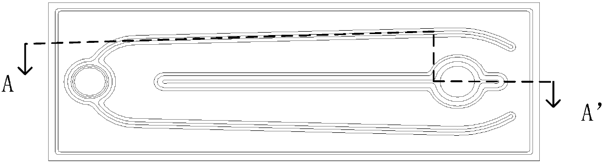
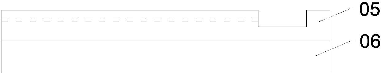
[0055] Specifically, such as figure 1 and figure 2 As shown, among them, figure 1 It is a schematic top view structural diagram of an LED chip in the prior art; figure 2 for along figure 1 The cross-section of the line AA' in the middle is a schematic diagram of the LED chip structure after adding a current blocking layer in the prior art; the LED chip includes a substrate 06, an epitaxial structure 05 grown on the substrate 06, a current blocking layer 01, a transparent conductive Layer 02, metal electrodes (03A and 03B) and passivation protection layer 04, which mainly prevent electrons / holes from recombining under the metal electrode 03 by providing an insulating current blocking layer 01 under the met...


PUM


Abstract

The present application provides a light-emitting diode and a manufacturing method thereof. In the light-emitting diode manufacturing method provided in the present application, on the one hand, the passivation layer is located between the second metal electrode and the transparent conductive layer, and via holes are formed on the passivation layer, so that The second metal electrode and the transparent conductive layer are electrically connected through the via hole on the passivation layer under the finger of the second metal electrode, so that the current is expanded, thereby playing the role of the current blocking layer in the prior art, and then can The current blocking layer is removed, saving the material cost of the current blocking layer. On the other hand, due to the manufacturing method of the light emitting diode provided in the present application, the current blocking layer is removed, and at least one photolithography process of the current blocking layer can be reduced, thereby reducing the cost of the photolithography process and simplifying the process.

Description

technical field [0001] The invention relates to the field of optoelectronic technology, in particular to a light emitting diode and a manufacturing method thereof. Background technique [0002] Light Emitting Diode (LED) is a new generation of environmentally friendly light source to replace incandescent and fluorescent lamps. Compared with traditional lighting sources, LED has many advantages such as high efficiency, low energy consumption, long life, no pollution, small size, and rich colors. , are widely used in lighting, display and backlighting and other fields. However, because the existing LED chip still has the problem of low luminous efficiency, how to improve the luminous efficiency of the LED chip has become one of the most important topics in the field of scientific research today. [0003] A method of using a current blocking layer to improve the luminous efficiency of an LED chip is proposed in the prior art. However, adding a current blocking layer in the LE...

Claims


Application Information

Patent Timeline
Patent Type & Authority Applications(China)
IPC IPC(8): H01L33/00H01L33/38H01L33/44
CPCH01L33/44H01L33/0075H01L33/382H01L33/387H01L2933/0016H01L2933/0025
Inventor 魏振东周弘毅李俊贤吴奇隆刘英策
Owner XIAMEN CHANGELIGHT CO LTD
Why Eureka
Try Eureka