
Oxide insulator film and thin-film transistor

A thin film transistor and insulator technology, applied in the field of oxide insulator thin films and thin film transistors, can solve the problems of easy diffusion, unfavorable electrical properties of oxide semiconductor devices, serious Al diffusion, etc.

Active Publication Date: 2018-08-17
SOUTH CHINA UNIV OF TECH
View PDF10 Cites 2 Cited by
  • Summary
  • Abstract
  • Description
  • Claims
  • Application Information

AI Technical Summary

Problems solved by technology

Al 2 o 3 Although it has a high relative permittivity (~9) and bandgap width (7.3-7.8eV), and can still maintain an amorphous phase at a high annealing temperature, due to the small ionic radius of Al (0.053nm ), and the binding energy with oxygen is small (511kj / mol), which is prone to diffusion, especially the diffusion of Al in the device prepared by the solution method is relatively serious, which is detrimental to the electrical properties of the oxide semiconductor device

Method used


Image

  • Oxide insulator film and thin-film transistor
  • Oxide insulator film and thin-film transistor
  • Oxide insulator film and thin-film transistor

Examples


Embodiment 1

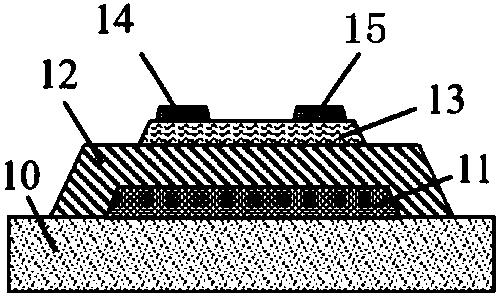
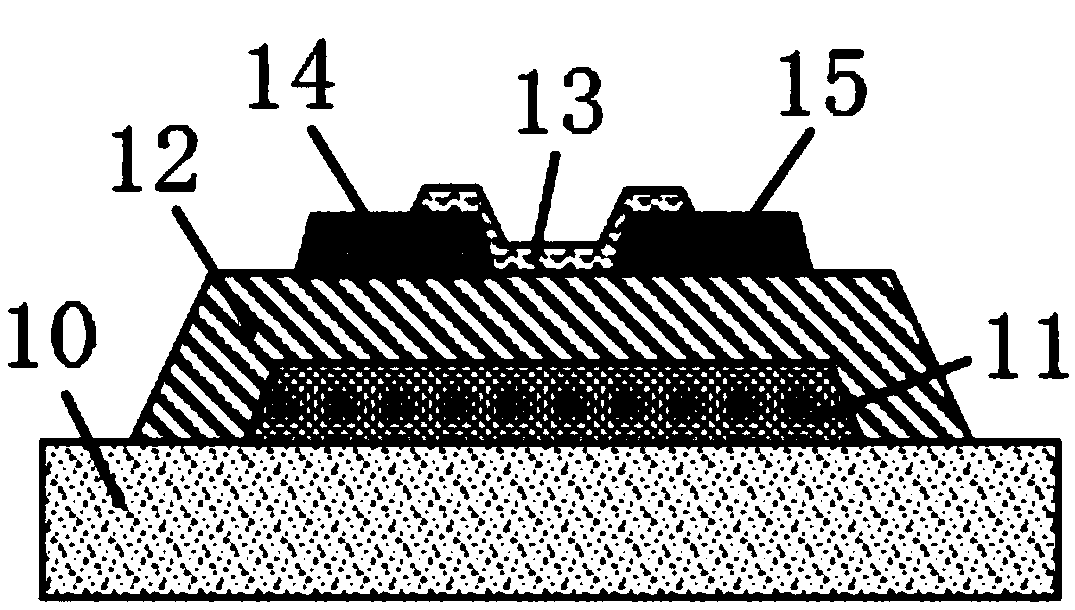
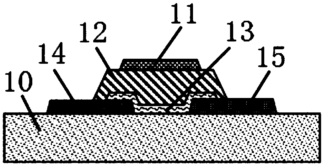
[0029] An oxide insulator film, the composition of which is M x al y Zr z o δ , M is a group IIIB metal element, 0.01≤x≤0.5, 0.3≤z<0.99, x+y+z=1, 0<δ≤2.

[0030] The film thickness is 2-1000nm. The thin film is prepared by vacuum method. Specifically, the vacuum method may be any one of single-target magnetron sputtering, multi-target magnetron sputtering, plasma-enhanced chemical vapor deposition, and atomic layer deposition.

[0031] The bandgap width of the film is greater than 4.5eV, which can effectively increase the injection barrier, and the breakdown field strength is greater than 3MV / cm, which can effectively reduce the breakdown probability. The thin film serves as an insulating layer for thin film transistors.

[0032] Compared with the traditional insulating film material, the M of the present embodiment x al y Zr z o δ Oxide insulator thin films have the following excellent technical effects:

[0033] (1) The film still maintains an amorphous phase at a...

Embodiment 2

[0040] An oxide insulator thin film, the other features are the same as those in Embodiment 1, except that M is the element Sc or Y.

[0041] M in this example x al y Zr z o δ In the oxide insulator film, M is the element Sc or Y. Since the oxide of Sc or Y has more negative fixed charges, it can shield part of the gate electric field, thereby offsetting the threshold voltage shift caused by the increase of carrier concentration. , which effectively avoids the problem of increased carrier concentration due to donor doping caused by the diffusion of Zr into oxide semiconductors (such as InZnO, InGaZnO, etc.).

Embodiment 3

[0043] An oxide insulator thin film, other features are the same as in Embodiment 2, the difference is that the thin film is prepared by a solution method, and the solution method is one of spin coating, scraping coating, spray coating and inkjet printing.

[0044]The oxide insulator thin film in this embodiment is prepared by a solution method. Compared with the vacuum method and other film preparation methods, the solution method has the advantages of low cost and easy control of the ratio. The solution method can simply adjust the composition of the precursor to control the ratio of the film components to achieve the control of the negative charge density in the insulating layer. Purpose, so that the threshold voltage of the thin film transistor can be adjusted more effectively.


PUM


Abstract

An oxide insulator film has a component of MxAlyZrzOdelta, wherein M is an element Sc or Y, 0.01<=x<=0.5, 0.3<=z<0.99, x+y+z=1, 0<delta<=2, and the thickness is 2-1000 nm. The oxide insulator film isprepared according to a vacuum method or a solution method and is used as an insulating layer of the thin-film transistor. The thin-film transistor is provided with a gate electrode, a channel layer,an insulating layer between the gate electrode and the channel layer, a source electrode and a drain electrode, wherein the source electrode and the drain electrode are connected with two ends of thechannel layer. The insulating layer is the oxide insulator film. The oxide insulator film has relatively large forbidden band width and is not sensitive to water, oxygen and carbon dioxide in air. Lowsurface roughness is realized. Low interface carrier trap density with an oxide semiconductor contact interface is realized. Therefore the thin-film transistor with the oxide insulator film as the insulator has advantages of high carrier mobility and stable electric performance.

Description

technical field [0001] The invention relates to the technical field of semiconductors, in particular to an oxide insulator thin film and a thin film transistor. Background technique [0002] In recent years, oxide thin-film transistors (TFTs) have attracted extensive attention and research because of their potential applications in flat panel displays, electronic labels, and sensors. Since the TFT device is a thin-film structure, the dielectric constant, crystallinity, density, bandgap width and thickness of the insulating layer have an important impact on the electrical properties of the transistor. At present, a large part of oxide TFT devices use thermally oxidized SiO 2 as an insulating layer, but SiO 2 The relative dielectric constant of the device is low (~4), and the device often needs a higher driving voltage in order to have a higher output current to meet the driving requirements. In many applications, for energy saving and safety considerations, the general requ...

Claims


Application Information

Patent Timeline
Patent Type & Authority Applications(China)
IPC IPC(8): H01L29/51H01L29/786
CPCH01L29/517H01L29/7869
Inventor 兰林锋李育智彭俊彪
Owner SOUTH CHINA UNIV OF TECH
Learn More