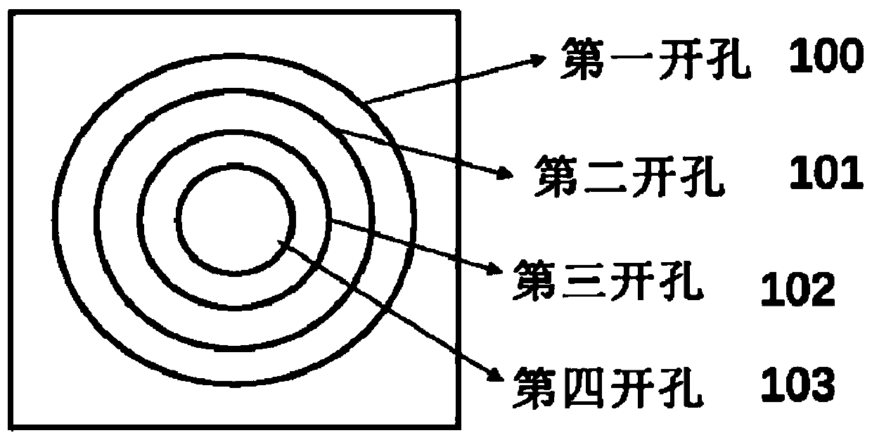
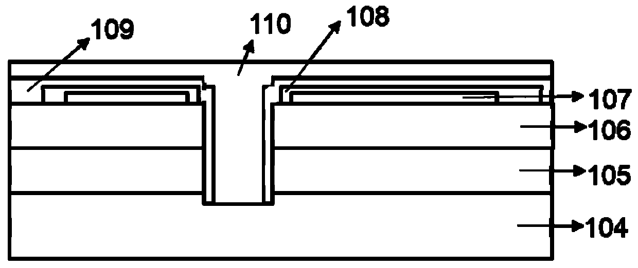
A method for reducing the voltage of a 3D through-hole superstructure LED chip by anaerobic dry etching in a hole

An LED chip, dry etching technology, applied in circuits, electrical components, semiconductor devices, etc., can solve the problems of passivation layer corrosion failure, inability to progress, LED chip voltage increase, etc., to achieve improved current distribution uniformity, good quality The effect of rate improvement and light efficiency improvement

Active Publication Date: 2020-02-18
SOUTH CHINA UNIV OF TECH
View PDF3 Cites 0 Cited by
  • Summary
  • Abstract
  • Description
  • Claims
  • Application Information

AI Technical Summary

Problems solved by technology

Wet etching has severe lateral corrosion, and the photoresist cannot prevent the ultrasonically oscillating BOE solution from passing through the undercut edge of the photoresist and penetrating laterally into the SiO2 passivation layer covering the sidewall of the N-hole, resulting in corrosion failure of the passivation layer , if no ultrasound is added, the SiO2 passivation layer in contact with n-GaN at the bottom cannot be etched away because of the capillary phenomenon generated by the BOE solution in the micron-sized through hole
Although dry etching does not have the lateral corrosion problem faced by wet methods, the commonly used dry etching gas for etching SiO2 is generally O 2 / SF 6 Mixed gas and oxygen plasma can accelerate the etching rate, but there are two obvious defects as follows. One is that the oxygen plasma will also etch the photoresist while etching SiO2, and the etching ratio of SiO2 / photoresist If it is relatively small, it will cause the photoresist to be too thin to be lower than the minimum critical thickness required for lift-off stripping, and the lift-off process cannot be performed; the second is that the n-GaN exposed at the bottom of the hole will be exposed during the etching process of oxygen plasma Oxidation to form Ga 2 o 3 , which is a weak n-type high-resistance oxide, which forms a higher potential barrier on the surface, resulting in poor ohmic contact between the metal and n-GaN, which in turn causes the chip voltage to rise
Whether it is the current dry etching or wet etching process, it will cause the SiO2 in the hole to be etched uncleanly or form a high-resistance oxide, which will cause the voltage of the corresponding LED chip to increase and the electrical yield to decrease. Therefore, the above problems can be solved. It is the only way to realize the preparation of high-performance, high-yield 3D through-hole superstructure LED chips, and also the only way to realize high-power, super-drive LED lighting technology

Method used


Image

  • A method for reducing the voltage of a 3D through-hole superstructure LED chip by anaerobic dry etching in a hole
  • A method for reducing the voltage of a 3D through-hole superstructure LED chip by anaerobic dry etching in a hole
  • A method for reducing the voltage of a 3D through-hole superstructure LED chip by anaerobic dry etching in a hole

Examples


Embodiment 1

[0053] A method for reducing the voltage of a 3D through-hole superstructure LED chip by anaerobic dry etching in a hole, comprising the following preparation steps:

[0054] (1) Provide a silicon substrate, and epitaxially grow LED epitaxial wafers on the silicon substrate, including n-type doped GaN films grown on silicon substrates, and InGaN / GaN multiple quantum wells grown on n-type doped GaN films , p-type doped GaN films grown on InGaN / GaN multiple quantum wells. The Si substrate has a (111) plane as an epitaxial plane. The thickness of the n-type doped GaN film is 1.8um; the InGaN / GaN multi-quantum well is 10 cycles of InGaN well layer / GaN barrier layer, wherein the thickness of the InGaN well layer is 5nm, and the thickness of the GaN barrier layer is 14nm; The thickness of the p-type doped GaN film is 250nm;

[0055] (2) Use the magnetron sputtering process to sputter nano-Ag-based reflectors on the surface of the LED epitaxial wafer, the sputtering power is 4.5kW,...

Embodiment 2

[0070] A method for reducing the voltage of a 3D through-hole superstructure LED chip by anaerobic dry etching in a hole, comprising the following preparation steps:

[0071] (1) Provide a Cu substrate, and epitaxially grow LED epitaxial wafers on the Cu substrate, including n-type doped GaN films grown on Cu substrates, and InGaN / GaN multiple quantum wells grown on n-type doped GaN films , p-type doped GaN films grown on InGaN / GaN multiple quantum wells. The Cu substrate has a (111) plane as an epitaxial plane. The thickness of the n-type doped GaN film is 3.5um; the InGaN / GaN multi-quantum well is 6 cycles of InGaN well layer / GaN barrier layer, wherein the thickness of InGaN is 6nm, and the thickness of GaN barrier layer is 11nm; The thickness of the p-type doped GaN film is 400nm;

[0072] (2) Nano-Ag-based reflectors were evaporated on the surface of the LED epitaxial wafer by electron beam evaporation process, the evaporation rate was 2 Å / s, and the evaporation temperat...


PUM

PropertyMeasurementUnit
thicknessaaaaaaaaaa
thicknessaaaaaaaaaa
thicknessaaaaaaaaaa

Abstract

The invention discloses an in-hole oxygen-free dry etching method for reducing the voltage of an LED chip of a 3D through hole superstructure. The method comprises that an n type doped GaN layer, an InGaN / GaN multi-quantum well layer and a p type doped GaN layer are prepared on an epitaxial substrate. A nanometer Ag-based reflector, reflector protective layer, N MESA holes and an insulating layerare prepared in the surface of an LED epitaxial wafer, and n-pad circular holes are formed; SiO2 in the n-pad circular holes are etched in an oxygen-free drying method, the holes are filled with N metal electrodes, and bonding layer metal is prepared; and an old growth substrate is peeled, an MESA cutting channel, a passivation layer PA, a P electrode pattern and P electrode metal are prepared toform the LED chip. The etching ratio of SiO2 to photoresist is controlled to solve the problem that the voltage of the LED chip of the 3D through hole superstructure is too high. The yield rate of thedriving voltage of the whole LED wafer is improved greatly, and the average of in-wafer voltage can be reduce to a value lower than 3.0V.

Description

technical field [0001] The invention relates to the field of LED manufacturing, in particular to a method for reducing the voltage of a 3D through-hole superstructure LED chip by in-hole anaerobic dry etching. Background technique [0002] With the gradual application of LEDs in the field of lighting, the market has higher and higher requirements for the light efficiency of white LEDs. 3D through-hole superstructure LED chips have come into people's field of vision. 3D through-hole superstructure LED chips are made by photolithography The method of dry etching drills holes on the surface of the epitaxial wafer p-GaN, the holes extend to n-GaN, and deposits metal electrodes in the holes. Therefore, the hole is surrounded by a 3D level of current expansion, which is far superior to the 2D current expansion of the vertical linear structure; uniformly distributed holes can improve the 2D current expansion ability of the n-GaN surface; In addition to the advantages of the linear...

Claims


Application Information

Patent Timeline
Patent Type & Authority Patents(China)
IPC IPC(8): H01L33/62H01L33/04H01L33/00
CPCH01L33/005H01L33/04H01L33/62
Inventor 李国强张云鹏
Owner SOUTH CHINA UNIV OF TECH
Why Eureka
Try Eureka