Solar cell and preparation method thereof

A solar cell and battery technology, applied in the field of solar cells, can solve problems such as reducing the electrical performance of solar cells, and achieve the effects of reducing contact area, increasing open circuit voltage, and increasing open circuit voltage

Active Publication Date: 2018-08-10
SHUNDE SYSU INST FOR SOLAR ENERGY
View PDF5 Cites 1 Cited by
  • Summary
  • Abstract
  • Description
  • Claims
  • Application Information

AI Technical Summary

Problems solved by technology

thereby reducing the electrical performance of the solar cell

Method used


Image

  • Solar cell and preparation method thereof
  • Solar cell and preparation method thereof
  • Solar cell and preparation method thereof

Examples


Embodiment 1

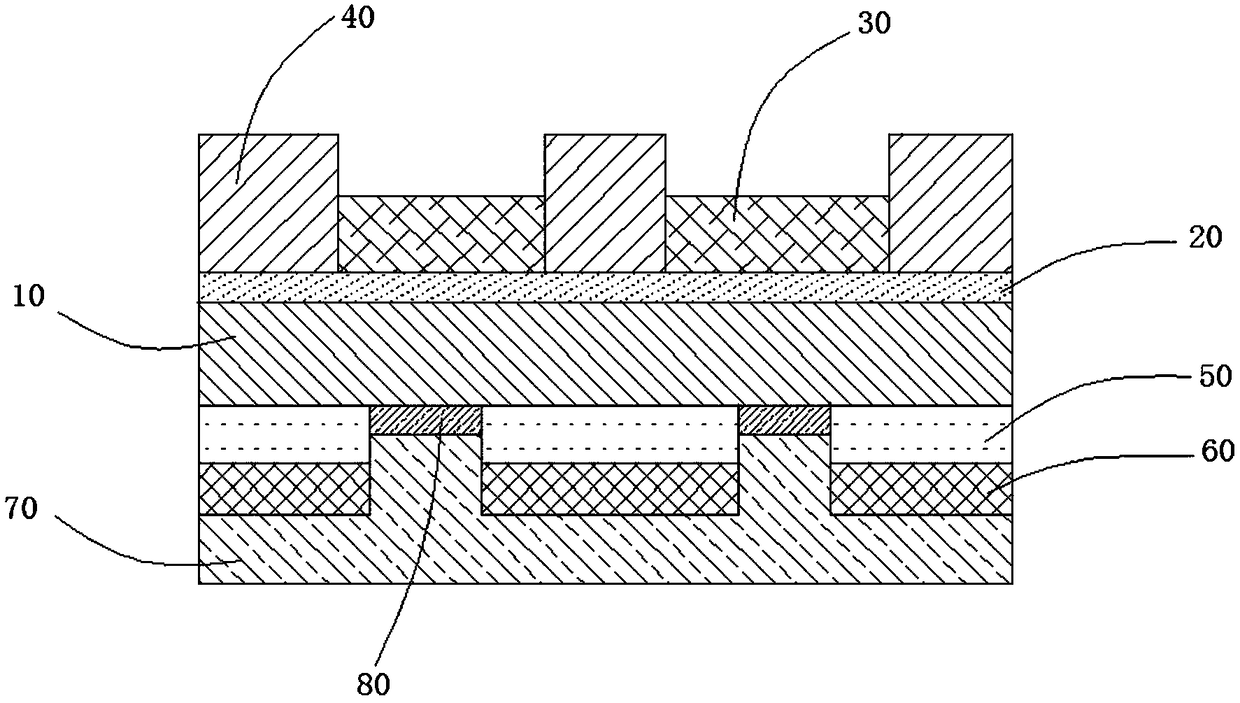
[0059] Such as figure 1 As shown, this embodiment is a solar cell, which includes the following parts:

[0060] 1) P-type silicon wafer 10: resistivity 2Ω·cm, as an absorption layer, converts the photons that meet the conditions into electrons, the size of the P-type silicon wafer is 2×2cm 2 ;

[0061] 2) n+ diffusion layer 20: also known as emitter, its main function is to form a p-n junction with p-Si to selectively transport electrons, with a depth of about 0.5μm, using POCl 3 As a phosphorus source, it is prepared by diffusion in a tube furnace;

[0062] 3) Silicon nitride anti-reflection film 30: prepared by PECVD deposition, with a thickness of about 75nm;

[0063] 4) Negative electrode 40: obtained by screen printing and high-temperature sintering, used to transport carriers;

[0064] 5) Al 2 O 3 Passivation layer 50: prepared by an atomic layer deposition method, with a thickness of about 5 nm, used to passivate p-type silicon wafers;

[0065] 6) Silicon nitride layer 60: prepare...

Embodiment 2

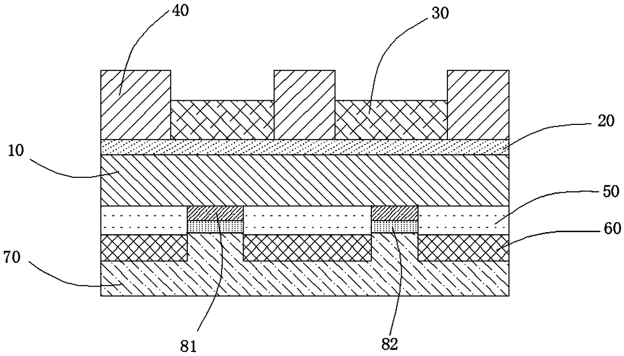
[0069] Such as figure 2 As shown, this embodiment is a solar cell. The difference from Embodiment 1 is that the high work function semiconductor material layer in this embodiment is two layers, which are divided into a first high work function semiconductor material layer 81 and a first high work function semiconductor material layer 81. Two high work function semiconductor material layers 82, wherein the first high work function semiconductor material layer 81 is 9 nm-V 2 O 5 , The second high work function semiconductor material layer 82 is 3nm-WO 3 . The high work function semiconductor material layer in this embodiment is denoted as 9nm-V 2 O 5 / 3nm-WO 3 , The other parts are the same as in Example 1.

Embodiment 3

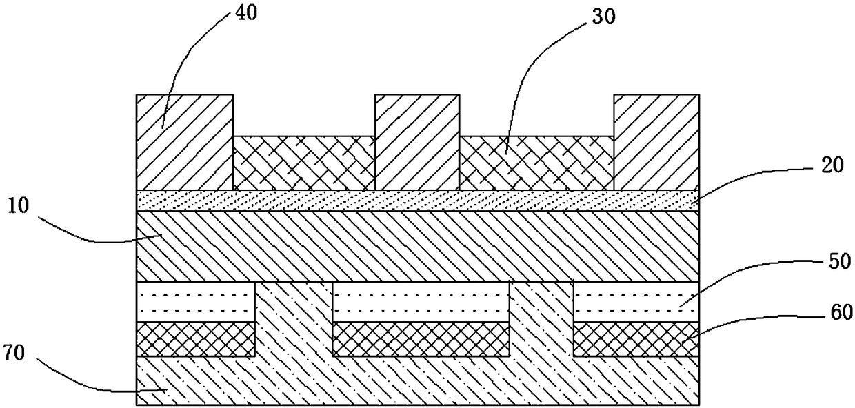
[0071] This embodiment is a solar cell. Compared with Embodiment 2, the difference is that the high work function semiconductor material layer is different. The high work function semiconductor material layer in this embodiment is 9nm-V 2 O 5 / 6nm-WO 3 , The other parts are the same as in Example 2.


PUM


Abstract

The present invention provides a solar cell and a preparation method thereof, and relates to the technology field of solar cells. The solar cell comprises a cell matrix, a passivating film and a backelectrode. The passivating film is located between the cell matrix and the back electrode, the passivating film is provided with an opening area, and the opening area is internally provided with a high-work-function semiconductor material layer which is located between the cell matrix and the back electrode. The solar cell is employed to relieve the technical problem that there is a high recombination region in a local contact solar cell to cause decreasing of the cell performances in the prior art and achieve the technical effects on reduction of the cell recombination region and improvementof the cell electrical performances in the prior art.

Description

Technical field [0001] The present invention relates to the technical field of solar cells, in particular to a solar cell and a preparation method thereof. Background technique [0002] Partial contact solar cells are also called PERC solar cells. The cells of this structure currently use Al 2 O 3 / SiNx laminated dielectric passivation film to passivate the back of the battery, due to Al 2 O 3 With negative charge, it can simultaneously achieve chemical passivation and field effect passivation of dangling bonds on the back side. However, because the laminated dielectric film is a non-conductive thin film, it needs to be partially laser-grooved, and then metallized by screen printing and high-temperature sintering. Although this method is currently a commercialized high-efficiency solar cell manufacturing technology, it can achieve a conversion efficiency greater than 21%. In the current industrialized PERC solar cell, the front side uses a silicon nitride anti-reflection film to ...

Claims


Application Information

Patent Timeline
Patent Type & Authority Applications(China)
IPC IPC(8): H01L31/068H01L31/0216H01L31/0224H01L31/18
CPCH01L31/02167H01L31/022441H01L31/068H01L31/1804H01L31/1868Y02E10/547Y02P70/50
Inventor 王学孟刘宗涛吴伟梁包杰
Owner SHUNDE SYSU INST FOR SOLAR ENERGY
Why Eureka
Try Eureka