High-k dielectric trench lateral double-diffused metal oxide wide bandgap semiconductor field effect transistor and method of making the same

A technology of lateral double-diffusion and field-effect transistors, which is applied in the field of lateral double-diffusion metal oxide semiconductor field-effect transistors and its production, can solve the problem of few technologies for optimizing the vertical electric field of devices, and achieve the optimization of vertical electric field distribution, performance improvement, Optimize the effect of contradictory relationship

Active Publication Date: 2020-08-21
XIDIAN UNIV
View PDF4 Cites 0 Cited by
  • Summary
  • Abstract
  • Description
  • Claims
  • Application Information

AI Technical Summary

Problems solved by technology

In the design optimization process of lateral power devices such as LDMOS, with the optimization of surface electric field terminal technology, including reduced surface electric field technology (Reduced Surface Field, referred to as RESURF), field plate (Field Plate, referred to as FP) technology, lateral variable doping ( With the application of technologies such as Variation of Lateral Doping (VLD for short), the surface electric field of lateral power devices has been optimized to a certain extent, but there are relatively few technologies for optimizing the vertical electric field of devices.

Method used


Image

  • High-k dielectric trench lateral double-diffused metal oxide wide bandgap semiconductor field effect transistor and method of making the same

Examples


Embodiment Construction

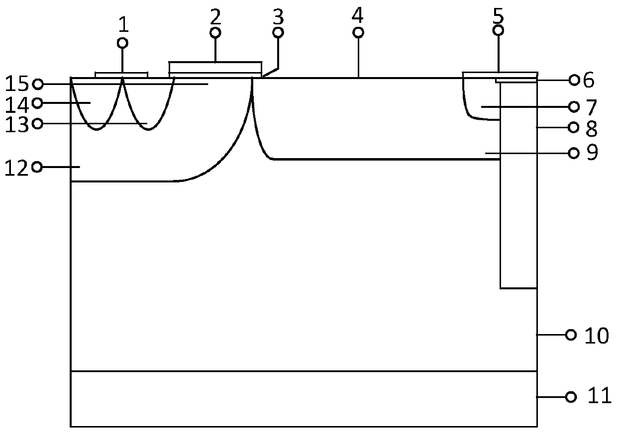
[0043] Such as figure 1 As shown, the high-K dielectric trench lateral double-diffused metal oxide wide bandgap semiconductor field effect transistor of the present invention includes:

[0044] A substrate 11 of a wide bandgap semiconductor material (such as gallium nitride, silicon carbide or diamond) (the doping concentration of the substrate is 1×10 13 cm -3 ~1×10 15 cm -3 );

[0045] an epitaxial layer 10 grown on a substrate 11;

[0046] A base region 12 and a drift region 9 formed on the epitaxial layer 10;

[0047] A source region 13 and a channel 15 formed on one side of the base region 12 adjacent to the drift region 9, and a drain region 7 formed on the other side of the drift region 9;

[0048] a channel substrate contact 14 formed outside the source region 13 in the base region;

[0049] The source electrode 1 formed by shorting the contact surface between the source region and the channel substrate;

[0050] A gate insulating layer 3 and a gate electrode 2...


PUM

PropertyMeasurementUnit
relative permittivityaaaaaaaaaa

Abstract

The invention provides a lateral double-diffused metal oxide wide-gap semiconductor field effect transistor (LDMOS) with a high-K dielectric (High-K Dielectric Pillar, HK) trench and a manufacturing method thereof. The device mainly forms a deep groove high-K dielectric layer at the drain end of the device, the lower end of the high-K dielectric layer goes deep into the epitaxial layer on the device substrate, and the upper end is connected with the drain electrode on the device surface. When the device is turned off, the uniform electric field of the HK dielectric trench reduces the peak high electric field generated by the cylindrical junction under the device drain, optimizes the longitudinal electric field distribution of the device, and improves the breakdown voltage of the device; moreover, the high-K dielectric Layer and wide bandgap semiconductor material substrate form a MIS capacitor structure, which can effectively assist in depleting the charge in the substrate when the device is turned off, effectively improving the doping concentration of the substrate under a certain withstand voltage of the device, that is, reducing the substrate resistivity.

Description

technical field [0001] The invention relates to the field of power semiconductor devices, in particular to a lateral double-diffused metal oxide semiconductor field effect transistor and a manufacturing method thereof. Background technique [0002] Wide bandgap semiconductor materials have the characteristics of large band gap, high critical breakdown electric field, high thermal conductivity and high electron saturation drift velocity, so they have very broad application prospects in the field of high-power, high-temperature and high-frequency power electronics. Lateral power devices have the advantages of easy integration, good thermal stability, good frequency stability, low power consumption, multi-subconduction, small power drive, and high switching speed, and are widely used in PIC (Power Integrated Circuit). At present, the lateral double-diffused metal-oxide-semiconductor field-effect transistor (LDMOS) with a wide bandgap semiconductor material (typically SiC) as th...

Claims


Application Information

Patent Timeline
Patent Type & Authority Patents(China)
IPC IPC(8): H01L29/78H01L29/40H01L21/336
CPCH01L29/402H01L29/66681H01L29/7816H01L29/0649H01L29/0653H01L29/1608H01L29/66068H01L29/66659H01L29/7835
Inventor 段宝兴曹震王彦东董自明杨银堂
Owner XIDIAN UNIV
Why Eureka
Try Eureka