High-voltage integrated power semiconductor device and manufacturing method thereof

A technology that integrates power and manufacturing methods. It is used in semiconductor/solid-state device manufacturing, semiconductor devices, and electrical components. It can solve problems such as difficulty in effectively improving device breakdown voltage, optimize vertical electric field distribution, improve vertical withstand voltage, and improve The effect of restriction

Pending Publication Date: 2022-07-29
UNIV OF ELECTRONICS SCI & TECH OF CHINA +1
View PDF9 Cites 0 Cited by
  • Summary
  • Abstract
  • Description
  • Claims
  • Application Information

AI Technical Summary

Problems solved by technology

However, in high-voltage LDMOS devices, the main factor limiting the withstand voltage of the device is the longitudinal breakdown, and it is difficult to effectively increase the breakdown voltage of the device by extending the length of the drift region.

Method used


Image

  • High-voltage integrated power semiconductor device and manufacturing method thereof
  • High-voltage integrated power semiconductor device and manufacturing method thereof
  • High-voltage integrated power semiconductor device and manufacturing method thereof

Examples


Embodiment 1

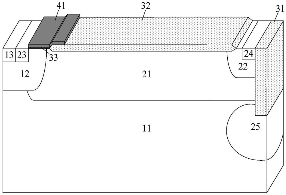
[0063] A high-voltage integrated power semiconductor device described in Embodiment 1, such as figure 1 shown, including:

[0064] First conductivity type substrate 11, second conductivity type drift region 21, first conductivity type well region 12, second conductivity type well region 22, first conductivity type heavily doped region 13, second conductivity type heavily doped region A23, the second conductive type heavily doped region B24, the second conductive type buried layer 25, the first dielectric layer 31, the second dielectric field oxide layer 32, the third dielectric gate oxide layer 33, and the control gate polysilicon electrode 41;

[0065] The first conductive type well region 12 is located on the left side of the second conductive type drift region 21 and is adjacent to it, and is connected to the first conductive type substrate 11 , and the second conductive type well region 22 is located in the second conductive type drift region. On the right side of and adj...

Embodiment 2

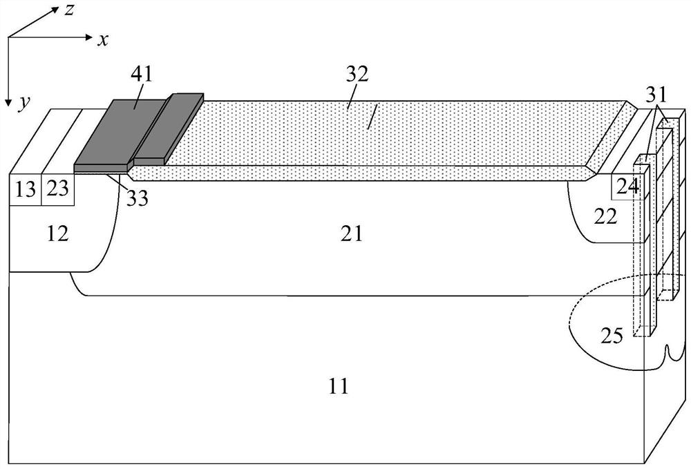
[0084] like figure 2 As shown, it is a schematic structural diagram of a high-voltage integrated power semiconductor device of Embodiment 2. The structure of this embodiment is different from that of Embodiment 1 in that the second conductive type buried layer 25 is connected to the second conductive type drift region 21, and its working principle is the same as Example 1 is basically the same.

Embodiment 3

[0086] like image 3 As shown, it is a schematic structural diagram of a high-voltage integrated power semiconductor device of Embodiment 3. The structure of this embodiment is different from that of Embodiment 1 in that the dielectric grooves are located in the heavily doped region B24 of the second conductivity type, and are arranged discretely in the Z direction. Its working principle is basically the same as that of Example 1.


PUM


Abstract

The invention provides a high-voltage integrated transverse semiconductor device and a manufacturing method thereof. Comprising a first conductive type semiconductor substrate, a first conductive type well region, a first conductive type semiconductor contact region, a second conductive type drift region, a second conductive type well region, a second conductive type semiconductor contact region, a second conductive type buried layer, a first dielectric layer, a second dielectric oxide layer, a third dielectric oxide layer and a polysilicon gate electrode, the second conductive type buried layer is located in the substrate and is formed through diffusion junction pushing after groove etching injection, and a groove is filled with a medium; when the second conductive type buried layer is in an off state, an electric field peak is introduced into the device body, and the longitudinal withstand voltage of the device is increased.

Description

technical field [0001] The invention belongs to the technical field of semiconductor process manufacturing, and relates to a high-voltage lateral power semiconductor device and a manufacturing method thereof Background technique [0002] The source, drain and gate of LDMOS devices are all on the surface of the chip, which is easy to integrate and is widely used in high-voltage integrated circuits and high-voltage power circuits. Because of its high input impedance, low loss, fast switching speed, wide safe operating area and easy integration, it can be used in many fields such as consumer electronics, automotive electronics, and LED displays. The power MOS device can be regarded as a composite structure in which a withstand voltage layer is introduced between the drain terminal and the quasi-drain terminal, that is, the drift region of the LDMOS device, so as to improve the breakdown voltage of the LDMOS device. However, in high-voltage LDMOS devices, the main factor limiti...

Claims


Application Information

Patent Timeline
Patent Type & Authority Applications(China)
IPC IPC(8): H01L29/06H01L29/78H01L21/336
CPCH01L29/7816H01L29/66681H01L29/0623
Inventor 章文通唐宁张科刘雨婷乔明何乃龙张森李肇基张波
Owner UNIV OF ELECTRONICS SCI & TECH OF CHINA
Why Eureka
Try Eureka