High voltage ldmos device

A device, high-voltage technology, applied in the field of high-voltage LDMOS devices, can solve the problems of not being able to take into account the forward demand of high withstand voltage and low on-resistance at the same time, and the long push-well time in the N-type drift region.

Active Publication Date: 2017-12-15
CSMC TECH FAB2 CO LTD
View PDF5 Cites 0 Cited by
  • Summary
  • Abstract
  • Description
  • Claims
  • Application Information

AI Technical Summary

Problems solved by technology

[0003] Since the existing technology cannot meet the forward requirements of high withstand voltage and low on-resistance at the same time, and because the N-type drift region takes a long time to push the well, it brings negative impacts on cost and energy consumption, it is necessary to propose new devices for process and Optimization and improvement of two aspects of the device

Method used


Image

  • High voltage ldmos device
  • High voltage ldmos device

Examples


Embodiment Construction

[0018] The present invention will be described in detail below in conjunction with the implementations shown in the drawings, but it should be noted that these implementations are not limitations of the present invention, and those of ordinary skill in the art based on the functions, methods, or structural changes made by these implementations Equivalent transformations or substitutions all fall within the protection scope of the present invention.

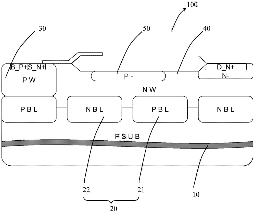
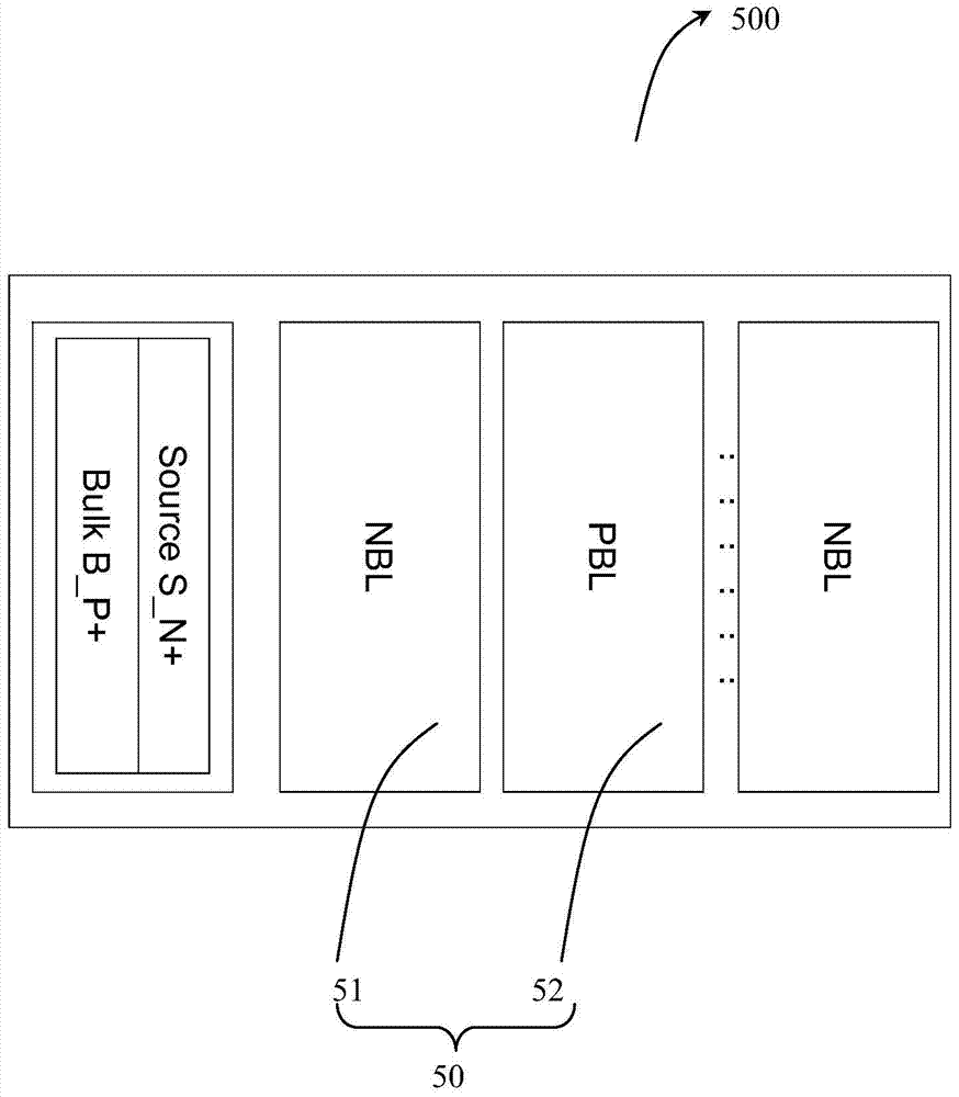
[0019] figure 1 is a schematic diagram of a high-voltage LDMOS device 100 in the first embodiment of the present invention, which includes a P-type substrate 10, a withstand voltage layer 20 located above the P-type substrate, a P-type channel region 30 located above the withstand voltage layer 20, and a N type drift region 40 and a P-type drop field layer 50 above the N-type drift region.

[0020] The P-type substrate 10 is used as the base of the high-voltage LDMOS device 100, and the P-type substrate is arranged below the volt...


PUM


Abstract

A high-voltage LDMOS (lateral double-diffused metal oxide semiconductor) device, including a P-type channel region, an N-type drift region, a voltage-resistant layer, and a P-type substrate at the bottom, and the voltage-resistant layer is located between the P-type substrate and the P-type substrate. Between the N-type drift region. The high-voltage LDMOS device of the present invention reduces the well-pushing time in the process by introducing the voltage-resistant layer, increases the cross-sectional area of ​​the current channel, improves the on-resistance, and improves the lateral voltage resistance by increasing the vertical voltage resistance.

Description

technical field [0001] The invention relates to the field of integrated circuits, in particular to a high-voltage LDMOS device. Background technique [0002] Due to the advantages of high voltage, low power consumption and high integration of BCD (bipolar-CMOS-DMOS) technology, there are more and more integrated circuits such as HVIC (high voltage integrated circuit) and SPIC (smart power integrated circuit) made of BCD technology. It is widely used in IPM (Intelligent Power Module) frequency conversion modules for motor drives, high-power LED lighting and white goods. The core device of BCD technology, UHV-NLDMOS (ultra-high voltage-N-type lateral double-diffused metal oxide semiconductor), has the highest development difficulty due to its high withstand voltage and low on-resistance, and major companies are competing to launch their own unique device structures. In order to obtain low on-resistance, a deep junction and high-concentration N-type (electronic type) drift reg...

Claims


Application Information

Patent Timeline
Patent Type & Authority Patents(China)
IPC IPC(8): H01L29/78H01L29/10
CPCH01L29/7816H01L29/0623H01L29/063H01L29/0878H01L29/1095H01L29/42368
Inventor 祁树坤
Owner CSMC TECH FAB2 CO LTD
Why Eureka
Try Eureka