High-k dielectric trench lateral superjunction double-diffused metal oxide element semiconductor field effect transistor and manufacturing method thereof

A field effect transistor and semiconductor technology, which is applied in the field of lateral superjunction double diffusion metal oxide semiconductor field effect transistor and its fabrication

Active Publication Date: 2020-08-21
XIDIAN UNIV
View PDF4 Cites 0 Cited by
  • Summary
  • Abstract
  • Description
  • Claims
  • Application Information

AI Technical Summary

Problems solved by technology

At present, there are few techniques for optimizing the vertical electric field of SJ-LDMOS devices

Method used


Image

  • High-k dielectric trench lateral superjunction double-diffused metal oxide element semiconductor field effect transistor and manufacturing method thereof
  • High-k dielectric trench lateral superjunction double-diffused metal oxide element semiconductor field effect transistor and manufacturing method thereof

Examples


Embodiment Construction

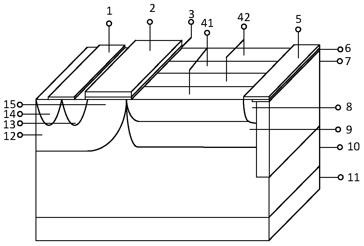
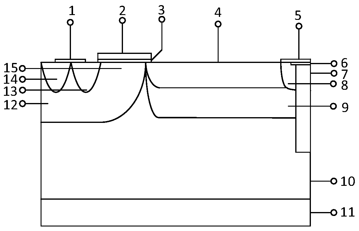
[0048] Such as figure 1 As shown, the lateral superjunction double-diffused metal oxide element semiconductor field effect transistor of the high-K dielectric trench proposed by the present invention includes:

[0049] A substrate 11 of elemental semiconductor material (such as silicon or germanium) (with a doping concentration of 1×10 13 cm -3 ~1×10 15 cm -3 );

[0050] an epitaxial layer 10 grown on a substrate;

[0051] The base region 12 and the buffer layer 9 formed on the epitaxial layer; the product of the doping concentration of the buffer layer and the thickness of the buffer layer satisfies the principle of charge balance to eliminate the substrate-assisted depletion effect; the doping concentration of the buffer layer is 1×10 14 cm -3 ~1×10 16 cm -3 ;

[0052] The super junction drift region 4 formed on the buffer layer is composed of several N columns 41 and P columns 42 arranged alternately; the doping concentration of the super junction drift region is 1...


PUM

PropertyMeasurementUnit
relative permittivityaaaaaaaaaa

Abstract

The invention provides a high-k dielectric (high-K dielectric pillar, HK) groove transverse super-junction double-diffused metal oxide element semiconductor field-effect tube (SJ-LDMOS) and a manufacturing method thereof. According to the invention, a high-k dielectric layer with a deep groove is formed in the drain terminal region of the SJ-LDMOS device. The upper end of the high-k dielectric layer is connected with a drain electrode and the lower end thereof penetrates through a super-junction drift region and a buffer layer to extend into an epitaxial layer above a substrate. The high-k dielectric layer with the deep groove and the substrate made of the element semiconductor material together form an MIS capacitor structure. When the device is turned off, the high-k dielectric layer isprovided with a uniform electric field. In this way, the electric field distribution in the body of the SJ-LDMOS device can be modulated. The longitudinal peak electric field at the drain terminal ofthe SJ-LDMOS device is reduced. The problem that a transverse LDMOS device is easily saturated along with the length breakdown voltage of the drift region of the device is solved. The contradiction between the breakdown voltage of the device and the specific on-state resistance is optimized.

Description

technical field [0001] The invention relates to the field of power semiconductor devices, in particular to a lateral superjunction double-diffused metal oxide semiconductor field effect transistor and a manufacturing method thereof. Background technique [0002] Lateral double-diffused MOS (Lateral Double-diffused MOS, referred to as LDMOS) as a representative of high voltage, low on-resistance lateral power devices are widely used in high-voltage integrated circuits (High Voltage Integrated Circuit, referred to as HVIC) and smart power integrated circuits ( Smart Power Integrated Circuit, referred to as SPIC). Super junction (Super Junction, referred to as SJ) technology can make it have a very low specific on resistance (Specific On Resistance, referred to as R) under a certain breakdown voltage (Breakdown Voltage, referred to as BV) ON,sp ), which is applied to LDMOS to form SJ-LDMOS structure, which breaks the limit relationship of traditional power MOS devices. Howeve...

Claims


Application Information

Patent Timeline
Patent Type & Authority Patents(China)
IPC IPC(8): H01L29/78H01L21/36H01L29/06
CPCH01L29/0615H01L29/0688H01L29/66477H01L29/7816
Inventor 段宝兴曹震杨鑫谢丰耘杨银堂
Owner XIDIAN UNIV
Why Eureka
Try Eureka