A progressive laser lift-off process for micron-sized sapphire substrates

A sapphire substrate, laser lift-off technology, applied in semiconductor devices, electrical components, circuits, etc., can solve the problems of reduced device process yield and self-reliability, increased device leakage, material damage, etc., and achieves the peeling process yield rate Improve, reduce process complexity, reduce the effect of high pressure nitrogen impact

Active Publication Date: 2020-05-22
XI AN JIAOTONG UNIV
View PDF5 Cites 0 Cited by
  • Summary
  • Abstract
  • Description
  • Claims
  • Application Information

AI Technical Summary

Problems solved by technology

At present, the most common laser lift-off processing method is to peel off the sapphire and epitaxial layer continuously and progressively along the horizontal or vertical direction. This method has a simple process and relatively low requirements for equipment hardware and programming, but laser irradiation When the epitaxial layer interface is decomposed due to the absorption of laser energy by the epitaxial layer, a large stress release and high-pressure nitrogen impact will be generated at the same time. The reciprocating continuous progressive processing in this direction will cause serious damage to the unstripped epitaxial functional area in the adjacent area. The impact of the impact can easily cause material damage, device failure or device leakage will be significantly aggravated, and eventually lead to a significant reduction in the process yield and reliability of the device

Method used


Image

  • A progressive laser lift-off process for micron-sized sapphire substrates
  • A progressive laser lift-off process for micron-sized sapphire substrates
  • A progressive laser lift-off process for micron-sized sapphire substrates

Examples


Embodiment 1

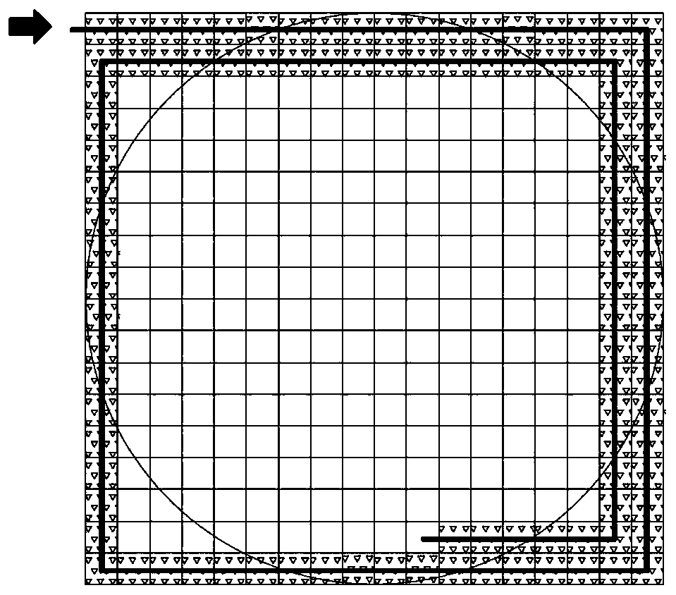
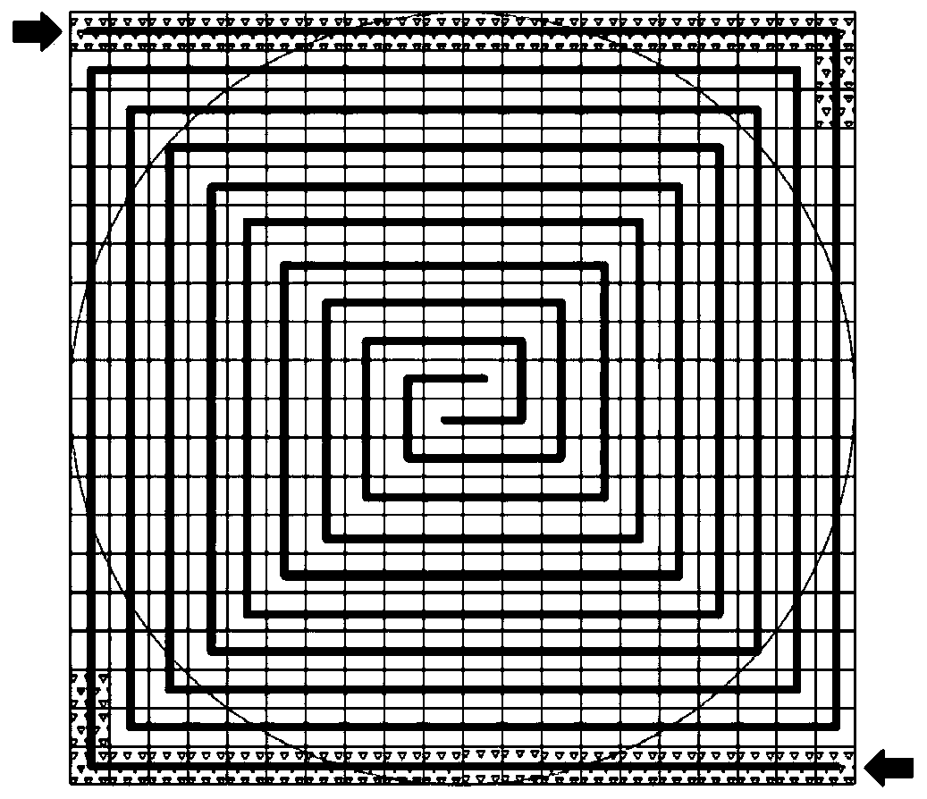
[0028] A progressive micron-scale sapphire substrate laser lift-off process provided by the present invention specifically includes the following steps:

[0029] (1) Firstly, the GaN LED epitaxial layer 101 is prepared on the sapphire substrate 100 by epitaxial growth method, and the total thickness of the epitaxial layer 101 is controlled at 5-10 microns; including the buffer layer Buffer layer, the unintentionally doped layer U- GaN, heavily doped N-GaN, multiple quantum wells MQW, electron blocking layer EBL, heavily doped P-GaN. The epitaxial growth method can be metal chemical vapor deposition, laser assisted molecular beam epitaxy, laser sputtering, or hydride vapor phase epitaxy. The deposited epitaxial film can be amorphous, polycrystalline, or single crystal structure. The sapphire substrate includes but is not limited to one of the mirror surface or micro-scale / nano-scale patterned sapphire substrate. The preferred solution is the mirror surface sapphire substrate ;...

Embodiment 2

[0034] A progressive micron-scale sapphire substrate laser lift-off process provided by the present invention specifically includes the following steps:

[0035] (1) First, an AlGaN epitaxial layer 101 is prepared on a sapphire substrate 100 by an epitaxial growth method, and the total thickness of the epitaxial layer 101 is controlled at 5-10 microns; including a buffer layer Buffer layer, an AlN layer, and a superlattice structure SL , heavily doped N-AlGaN, multiple quantum well MQW, P-AlGaN, heavily doped P-GaN contact layer. The epitaxial growth method can be metal chemical vapor deposition, laser assisted molecular beam epitaxy, laser sputtering, or hydride vapor phase epitaxy. The deposited epitaxial film can be amorphous, polycrystalline, or single crystal structure. The sapphire substrate includes but is not limited to one of the mirror surface or micron-scale / nano-scale patterned sapphire substrate. The preferred solution is a micron-scale pattern sapphire substrate...


PUM


Abstract

The invention discloses a progressive micron sapphire substrate laser stripping process. The process comprises the following steps: 1) the needed epitaxial layer grows on the surface of the sapphire substrate, and according to needs, the epitaxial layer is subjected to unit area division; 2) according to needs, a conductive insulated material is filled between the unit areas; 3) the epitaxial layer is bonded with a transfer substrate; and 4) according to a counter clockwise or clockwise direction, by using a single beam or double beam laser irradiation mode, point-by-point scanning is carriedout in an outward-to-inward linear progressive scanning mode, separation between the sapphire substrate and the epitaxial layer is realized, and good stripping effects are acquired.

Description

technical field [0001] The invention belongs to the field of high-precision laser processing, and in particular relates to a progressive micron-level sapphire substrate laser stripping process. Background technique [0002] Visible and ultraviolet light-emitting diodes (Light Emitting Diodes, referred to as LEDs) based on III-N material systems have gradually realized efficient light emission in infrared, red, green, blue, and ultraviolet bands since the 1960s. Since then, semiconductor lighting technology It has achieved rapid development, and the luminous efficiency of products has been continuously improved. It has begun to replace traditional lighting methods and become the mainstream technology in the market. At this stage, the LED application market has reached hundreds of billions of yuan. Therefore, III-N materials have very broad market development prospects. [0003] LEDs generally use sapphire material as the epitaxial substrate, and use metal organic chemical vap...

Claims


Application Information

Patent Timeline
Patent Type & Authority Patents(China)
IPC IPC(8): H01L21/78H01L21/86H01L33/00
Inventor 云峰郭茂峰
Owner XI AN JIAOTONG UNIV
Why Eureka
Try Eureka