Formation method of fin-type field-effect transistor

A technology of fin field effect transistors and fins, which is applied in the direction of electrical components, semiconductor/solid-state device manufacturing, circuits, etc., to achieve the effects of improving electrical performance, avoiding etching damage, and good morphology

Active Publication Date: 2017-12-19
SEMICON MFG INT (SHANGHAI) CORP +1
View PDF4 Cites 0 Cited by
  • Summary
  • Abstract
  • Description
  • Claims
  • Application Information

AI Technical Summary

Problems solved by technology

[0005] However, the performance of the fin field effect transistor formed by the prior art needs to be further improved

Method used


Image

  • Formation method of fin-type field-effect transistor
  • Formation method of fin-type field-effect transistor
  • Formation method of fin-type field-effect transistor

Examples


Embodiment Construction

[0031] It can be seen from the background art that the electrical performance of the fin field effect transistor formed in the prior art needs to be improved.

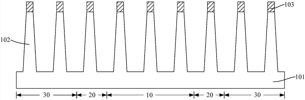
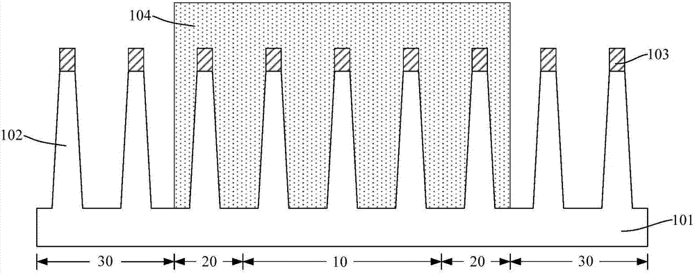
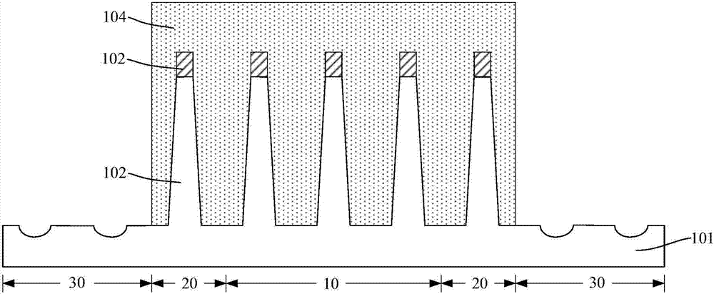
[0032] In the FinFET, the base usually includes an active area and an edge area adjacent to the active area, wherein the active area has a fin formed on the base, while the edge area has no fin on the base. Generally, the process steps of forming fins on the base of the active area include: firstly forming discrete fins on the base of the active area and the base of the edge area; then, forming a pattern covering the fins on the base of the active area layer; using the graphic layer as a mask, etching and removing the fins located on the base of the edge area; removing the graphic layer.

[0033] However, in the FinFET formed by the above method, the fins on the base of the active area will be damaged, resulting in changes in the shape and size of the fins, and the damage to the fins on the base of the active area clos...


PUM


Abstract

A formation method of a fin-type field-effect transistor is disclosed. The method comprises the following steps of providing a substrate including an effective area, first edge areas located on two sides of the effective area and a second edge area located on one side of the first edge area, and forming a fin portion on the substrate; forming a first graph layer covering an effective area fin portion and a first edge area fin portion; etching to remove a fin portion with a first thickness of the second edge area; forming a second graph layer covering the effective area fin portion; and taking the second graph layer as a mask layer, and etching to remove the fin portion with a second thickness of the first edge areas, wherein the second thickness is less than the first thickness. In the invention, through reducing an amount of the fin portion which is etched and removed on the substrate of the first edge areas next to the effective area, etching damages of the second graph layer are reduced or avoided so that the fin portion on the substrate of the effective area is prevented from exposing in an etching environment; the fin portion on the substrate of the effective area is prevented from being etched and damaged; and the fin portion on the substrate of the effective area possesses good morphology so that performance of the formed fin-type field-effect transistor is improved.

Description

technical field [0001] The invention relates to the technical field of semiconductor manufacturing, in particular to a method for forming a fin field effect transistor. Background technique [0002] With the continuous development of semiconductor process technology, the development trend of semiconductor process nodes following Moore's Law continues to decrease. In order to adapt to the reduction of process nodes, the channel length of MOSFET field effect transistors has to be continuously shortened. The shortening of the channel length has the advantages of increasing the die density of the chip and increasing the switching speed of the MOSFET field effect tube. [0003] However, as the channel length of the device is shortened, the distance between the source and the drain of the device is also shortened, so that the control ability of the gate to the channel becomes worse, and the gate voltage pinches off the channel. The difficulty is also increasing, making the pheno...

Claims


Application Information

Patent Timeline
IPC IPC(8): H01L21/336
CPCH01L29/66795
Inventor 李勇
Owner SEMICON MFG INT (SHANGHAI) CORP
Why Eureka
Try Eureka