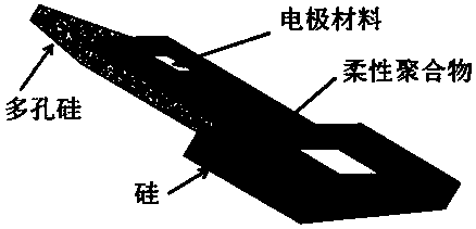
A neural electrode based on porous silicon and polymer, its manufacturing process and application
A porous silicon and polymer technology, applied in the field of neural electrodes, can solve problems such as brain tissue damage, and achieve the effects of low power consumption, low cost and small size
- Summary
- Abstract
- Description
- Claims
- Application Information
AI Technical Summary
Problems solved by technology
Method used
Image
Examples
Embodiment 1
[0043] This embodiment is a manufacturing method of a neural electrode device based on a porous silicon substrate:
[0044] 1. Production of porous silicon:
[0045] The manufacturing process of porous silicon is simple, and the preparation methods can be anode electrochemical corrosion method, hydrothermal corrosion method, and spark discharge method. Among them, the anodic electrochemical corrosion method is the most common and compatible with the MEMS process. In this method, platinum or graphite is used as an anode, and a patterned silicon wafer is used as a cathode to carry out electrocorrosion in HF solution. Or platinum or graphite is used as the anode and cathode, and the silicon wafer is suspended between the two plates. In the mixed solution of HF and ethanol, the electrochemical corrosion is realized under the action of the electric field. The corrosion rate and the aperture size of porous silicon are related to the doping concentration of single crystal silicon w...
Embodiment 2
[0053] The difference with Example 1 is: image 3 (a) and image 3 (b) can be omitted, and directly deposit isolation materials such as silicon nitride or polysilicon, and then perform patterning to open windows. The next step of porous silicon formation will enter the silicon substrate through the patterned window. However, it is isotropic corrosion at this time. etched porous silicon such as Figure 5 shown.
[0054] Subsequent methods and image 3 (f) and image 3 (g) Similarly, the next deep trench etch to define the device boundary will involve the etching of porous silicon. Since the dry etching rate of porous silicon depends on the porosity and the degree of oxidation of porous silicon, the etching conditions need to be strictly controlled. Finally, perform mechanical grinding on the back of the silicon wafer to reach the required device thickness.
Embodiment 3
[0056] Firstly, the functional layer of flexible polymer and metal is fabricated on the silicon substrate (same as image 3 (f)-(g)). The device and other areas are then protected with silicon nitride or silicon oxide or some other passivation layer. Open deep etch trenches (such as image 3 (h)). The final step is electrochemical etching of silicon to produce porous silicon. Since the formation of porous silicon is isotropic, the silicon below the polymer functional layer will eventually be corroded to form a porous silicon layer. Finally, perform mechanical grinding on the back of the silicon wafer to reach the required device thickness.
PUM
| Property | Measurement | Unit |
|---|---|---|
| porosity | aaaaa | aaaaa |
| porosity | aaaaa | aaaaa |
Abstract
Description
Claims
Application Information
 - R&D
- Intellectual Property
- Life Sciences
- Materials
- Tech Scout
- Unparalleled Data Quality
- Higher Quality Content
- 60% Fewer Hallucinations
Browse by: Latest US Patents, China's latest patents, Technical Efficacy Thesaurus, Application Domain, Technology Topic, Popular Technical Reports.
© 2025 PatSnap. All rights reserved.Legal|Privacy policy|Modern Slavery Act Transparency Statement|Sitemap|About US| Contact US: help@patsnap.com


