Semiconductor device

A semiconductor, conductive type technology, applied in the direction of semiconductor devices, electrical components, circuits, etc., can solve the problems of applying a large electric field, insulation breakdown of the gate insulating film, etc.

Inactive Publication Date: 2017-12-01
TOYOTA JIDOSHA KK
View PDF9 Cites 2 Cited by
  • Summary
  • Abstract
  • Description
  • Claims
  • Application Information

AI Technical Summary

Problems solved by technology

[0006] However, if the drift layer that should achieve low on-resistance is set to a high concentration in a MOSFET (Metallic Oxide Semiconductor Field Effect Transistor: Metal Oxide Semiconductor Field Effect Transistor) of a double gate structure, the bottom of the double gate structure will be Applying a large electric field may cause insulation breakdown of the gate insulating film
Especially in the case of a semiconductor device having a double-gate structure made of SiC, a larger electric field is applied to the bottom of the double-gate structure than when it is made of Si, and insulation breakdown of the gate insulating film may also occur. The problem

Method used


Image

  • Semiconductor device
  • Semiconductor device
  • Semiconductor device

Examples


no. 1 approach

[0020] A first embodiment of the present disclosure will be described. Here, although a SiC semiconductor device in which the semiconductor device is formed of SiC is taken as an example and described, the semiconductor device may be formed of other semiconductor materials such as Si.

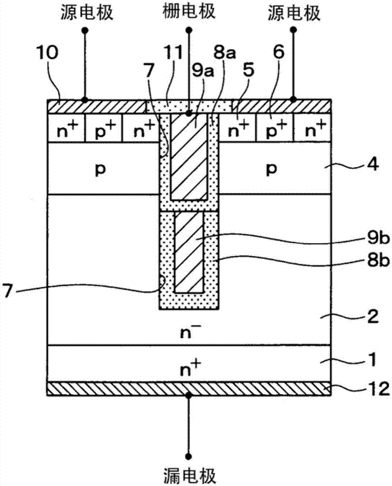
[0021] First, refer to figure 1 A SiC semiconductor device having a vertical MOSFET with an inverted trench gate structure according to this embodiment will be described. Also, while in figure 1 Only one cell with a vertical MOSFET is documented, but with figure 1 Semiconductors having the same structure as the illustrated vertical MOSFETs are arranged so that a plurality of cells are adjacent to each other. A unit mentioned here refers to the p + The center of the type contact region 6 starts from the p + The center of the type contact area 6.

[0022] Such as figure 1 As shown, using a SiC single crystal composed of n + type semiconductor substrate 1 to form a SiC semiconductor device...

no. 2 approach

[0043] A second embodiment of the present disclosure will be described. This embodiment has a structure capable of further increasing the breakdown voltage compared to the first embodiment, and since other points are the same as the first embodiment, only the parts different from the first embodiment will be described.

[0044] Such as figure 2 As shown, in the SiC semiconductor device of this embodiment, the p-type deep layer 3 is formed on both sides of the trench gate structure so as to be separated from the trench 7 by a predetermined distance. In the case of this embodiment, the p-type deep layer 3 is set parallel to the trench 7, that is, parallel to the figure 2 The direction perpendicular to the paper surface is a short grid shape in the longitudinal direction, and a plurality of p-type deep layers 3 are arranged in stripes, and trenches 7 are arranged between each p-type deep layer 3 . Specifically, on both sides of the position where the trench 7 is formed, a par...

no. 3 approach

[0048] A third embodiment of the present disclosure will be described. This embodiment also has a structure that can further increase the withstand voltage compared to the first embodiment, and since other points are the same as the first embodiment, only the parts that are different from the first embodiment will be described.

[0049] Such as image 3As shown, in the SiC semiconductor device of this embodiment, the p-type underlayer 20 is formed on the surface layer portion of the n-type drift layer 2 at the bottom of the trench gate structure. In the case of this embodiment, the p-type underlayer 20 is formed over the entire area of ​​the bottom of the trench 7, that is, in a image 3 The direction perpendicular to the paper surface is a short grid shape in the length direction. For example, p-type underlayer 20 is formed by ion-implanting p-type impurities in a state where the portion other than trench 7 is covered with a mask after trench 7 is formed. The p-type impuri...


PUM


Abstract

A semiconductor device that is provided with: a drain region (1) that is configured from a first or second conductive-type semiconductor; a drift layer (2) that is configured from the first conductive-type semiconductor; a base region (4) that is configured from the second conductive-type semiconductor; a source region (5) that is configured from a high concentration of the first conductive-type semiconductor; a contact region (6) that is configured from a high concentration of the second conductive-type semiconductor; a trench-gate structure that includes an upper-stage-side gate structure and a lower-stage-side gate structure; a source electrode (10) that is connected to the source region and the contact region; and a drain electrode (12) that is arranged on an undersurface side of the drain region. The upper-stage-side gate structure is arranged inside a trench (7) on an upper-stage side and has a first gate insulating film (8a) and a first gate electrode (9a). The lower-stage-side gate structure is arranged inside the trench (7) on a lower-stage side and has a second gate insulating film (8b), which is configured from an insulating material that has a high dielectric constant, and a second gate electrode (9b).

Description

[0001] Cross-reference of related applications [0002] This application is an invention based on Japanese Patent Application No. 2015-61395 for which it applied on March 24, 2015, and uses the description content here. technical field [0003] The present disclosure relates to a semiconductor device having a trench gate structure, and is particularly preferably applicable to a semiconductor device composed of silicon carbide (hereinafter referred to as SiC). Background technique [0004] Conventionally, a semiconductor device having a trench gate structure is known as a structure in which a channel density is increased in order to allow a large current to flow. In this trench gate structure, there is a structure in which another gate electrode is provided directly below the gate electrode (hereinafter, the upper side is referred to as the first gate electrode, and the lower side is referred to as the second gate electrode), and the The second gate electrode is connected to...

Claims


Application Information

Patent Timeline
Patent Type & Authority Applications(China)
IPC IPC(8): H01L29/78H01L29/06H01L29/12
CPCH01L29/78H01L29/0623H01L29/1095H01L29/1608H01L29/407H01L29/517H01L29/518H01L29/7397H01L29/7813H01L29/06H01L29/12H01L29/105H01L29/4236H01L29/512
Inventor 三村智博金村高司水野祥司杉本雅裕青井佐智子
Owner TOYOTA JIDOSHA KK
Why Eureka
Try Eureka