Inter-low-permittivity layer insulating film, and method for forming inter-low-permittivity layer insulating film

A technology of low dielectric constant layer and film-forming method, which is applied in coatings, circuits, electrical components, etc., can solve problems such as poor adhesion, reduced wiring reliability, and weak cohesive energy, and achieve barrier and tightness Improvement of compatibility, improvement of low dielectric constant, and suppression of insulation breakdown

Inactive Publication Date: 2013-01-30
NIPPON SANSO CORP +1
View PDF8 Cites 0 Cited by
  • Summary
  • Abstract
  • Description
  • Claims
  • Application Information

AI Technical Summary

Problems solved by technology

However, in the conventional low dielectric constant interlayer insulating film, there is a problem that the gas and metal barrier properties are poor due to many voids or voids.
In addition, conventional low dielectric constant interlayer insulating films have problems of weak cohesive energy and poor adhesion with films of other compositions.
[0015] If the barrier property or adhesion is poor, it will cause cracks in the insulating film, electromigration, stress migration, etc., and reduce the reliability of wiring
[0016] In this context, although an interlayer insulating film having properties such as low dielectric constant and suppression of insulating film cracking, electromigration, or stress migration is desired, it is actually difficult to achieve both, and effective and appropriate interlayer insulation cannot be provided. membrane

Method used


Image

  • Inter-low-permittivity layer insulating film, and method for forming inter-low-permittivity layer insulating film
  • Inter-low-permittivity layer insulating film, and method for forming inter-low-permittivity layer insulating film

Examples


Embodiment 1

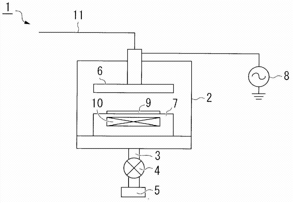
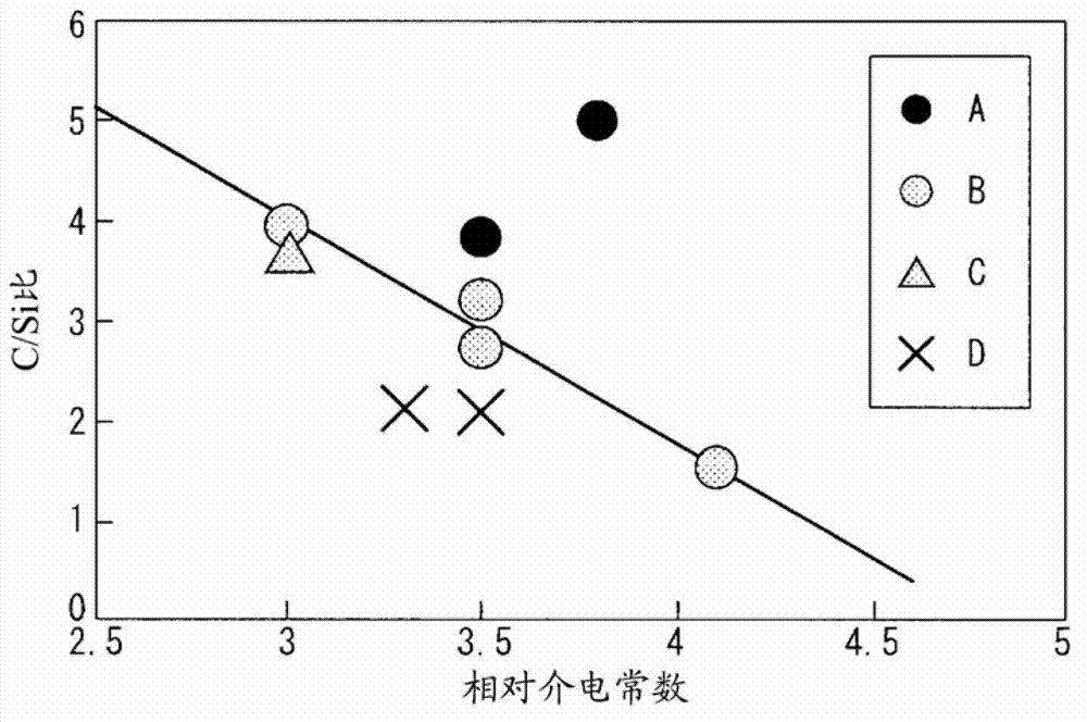
[0070] In Example 1, using isobutyltrimethylsilane (iBTMS) as the insulating film material, a SiCH film was formed under the conditions of a flow rate of 20 sccm, a pressure of 3 Torr, and a plasma output power of 550 W. As a result, a SiCH film with a relative dielectric constant of 3.5 was obtained . The ratio of carbon to silicon (C / Si ratio), porosity, barrier properties, and adhesiveness were evaluated, and the results are shown in Table 1.

[0071] From this result, it can be seen that in the low dielectric constant interlayer insulating film of Example 1, the C / Si ratio is large, and thus the porosity is small. In addition, it can be seen that the barrier properties are equal to those of known interlayer insulating films.

Embodiment 2

[0073] In Example 2, diisobutyldimethylsilane (DiBDMS) was used as the insulating film material, and the SiCH film was formed under the conditions of a flow rate of 20 sccm, a pressure of 3 Torr, and a plasma output power of 650 W. As a result, SiCH with a relative dielectric constant of 3.5 was obtained. membrane. The ratio of carbon to silicon (C / Si ratio), porosity, barrier properties, and adhesiveness were evaluated, and the results are shown in Table 1.

[0074] From this result, it can be seen that in the low dielectric constant interlayer insulating film of Example 2, the C / Si ratio is large, so the porosity is small. In addition, it can be seen that the barrier property is equal to that of a known interlayer insulating film, and the adhesiveness is superior to that of a known interlayer insulating film.

Embodiment 3

[0076] In Example 3, diisobutyldimethylsilane (DiBDMS) was used as an insulating film material, and a SiCH film was formed under the conditions of a flow rate of 20 sccm, a pressure of 3 Torr, and a plasma output power of 450 W. As a result, SiCH with a relative dielectric constant of 3.0 was obtained. membrane. The ratio of carbon to silicon (C / Si ratio), porosity, barrier properties, and adhesiveness were evaluated, and the results are shown in Table 1.

[0077] From this result, it can be seen that in the low dielectric constant interlayer insulating film of Example 3, the C / Si ratio is large, so the porosity is small. In addition, it can be seen that although the barrier property is slightly inferior to that of the known interlayer insulating film, the adhesion property is excellent.


PUM

PropertyMeasurementUnit
thicknessaaaaaaaaaa
relative permittivityaaaaaaaaaa

Abstract

Disclosed is an inter-low-permittivity layer insulating film which is formed by means of the plasma CVD method, contains at least carbon and silicon, and has a carbon to silicon ratio of 2.5 or more and a relative permittivity of 3.8 or less. Also disclosed is a method for forming an inter-low-permittivity layer insulating film which involves a step for forming an insulating film material containing at least carbon and silicon into a film by means of the plasma CVD method, wherein the aforementioned insulating film material has a carbon to silicon ratio of 2.5 or more and a relative permittivity of 3.8 or less without using hydrocarbon when said insulating film material is used to form an inter-low-permittivity layer insulating film.

Description

technical field [0001] The application relates to a low dielectric constant interlayer insulating film and a method for forming a low dielectric constant interlayer insulating film. [0002] This application claims priority based on Japanese Patent Application No. 2010-044263 for which it applied in Japan on March 1, 2010, and uses the content here. Background technique [0003] In recent years, with the high integration of semiconductor devices, the wiring layer has been miniaturized. However, it has been pointed out that if a finer wiring layer is used, the influence of signal delay in the wiring layer increases, which hinders the high speed of signal transmission. problem of transformation. This signal delay is proportional to the resistance of the wiring layer and the capacitance between the wiring layers. Therefore, in order to increase the speed, it is required to lower the resistance of the wiring layer and to reduce the capacitance between the wiring layers. [000...

Claims


Application Information

Patent Timeline
Patent Type & Authority Applications(China)
IPC IPC(8): H01L21/314C23C16/42C23C16/509H01L21/205H01L21/768H01L23/522
CPCH01L21/02167H01L21/02274H01L21/02211C23C16/30C23C16/50H01L21/02203
Inventor 清水秀治永野修次大桥芳加田武史菅原久胜
Owner NIPPON SANSO CORP
Why Eureka
Try Eureka