Image forming apparatus using amorphous silicon photoconductor
A technology of amorphous silicon and photoreceptors, which is applied in the electrical recording process using charge patterns, equipment and optics for electric recording processes using charge patterns, and can solve problems such as reduced withstand voltage performance, reduction, and destruction of insulation
- Summary
- Abstract
- Description
- Claims
- Application Information
AI Technical Summary
Problems solved by technology
Method used
Image

Examples
no. 1 approach
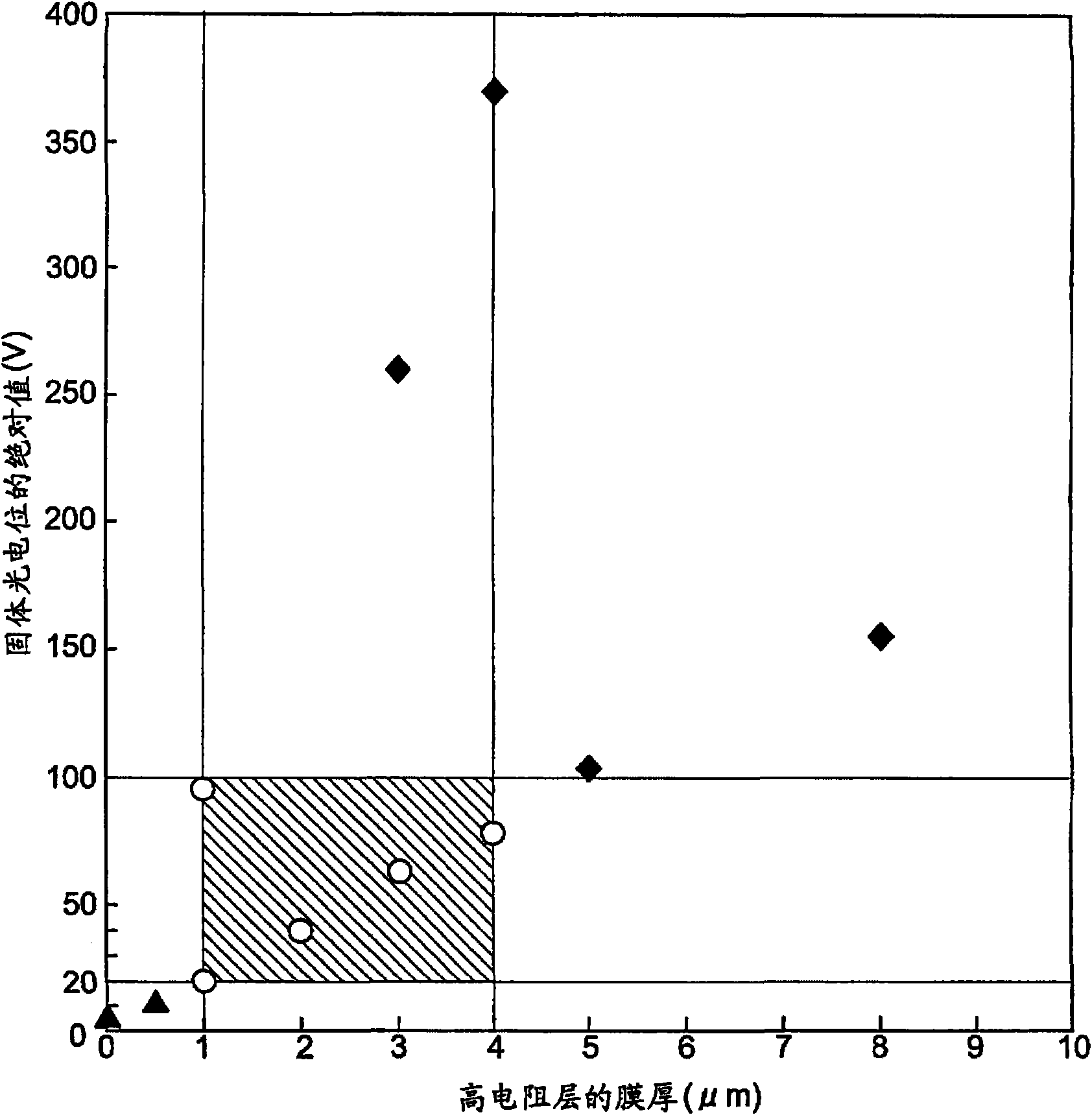
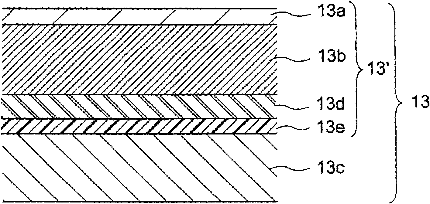
[0038] The image forming apparatus shown in the first embodiment has a photosensitive layer on a substrate, and the photosensitive layer is amorphous in which a high-resistance layer, a charge injection preventing layer, a photoconductive layer, and a surface protection layer are sequentially stacked on the substrate. A silicon photoreceptor, the amorphous silicon photoreceptor is installed in the image forming section. In this amorphous silicon photoreceptor, as figure 1 As shown, the film thickness of the high resistance layer is in the range of 1-4 μm, the film thickness of the photosensitive layer is in the range of 15-25 μm, and the absolute value of the solid photoelectric potential of the photosensitive layer is in the range of 20-100V Inside.
[0039] Each constituent element of the image forming apparatus of the first embodiment will be specifically described below.
[0040] 1. Basic structure
[0041] The image forming apparatus of the present embodiment includes ...
no. 2 approach
[0156] The second embodiment is an image forming method using the image forming apparatus described in the first embodiment. Hereinafter, the image forming method of the second embodiment will be described by taking a full-color image forming method using a full-color image forming apparatus as an example and focusing on differences from the first embodiment.
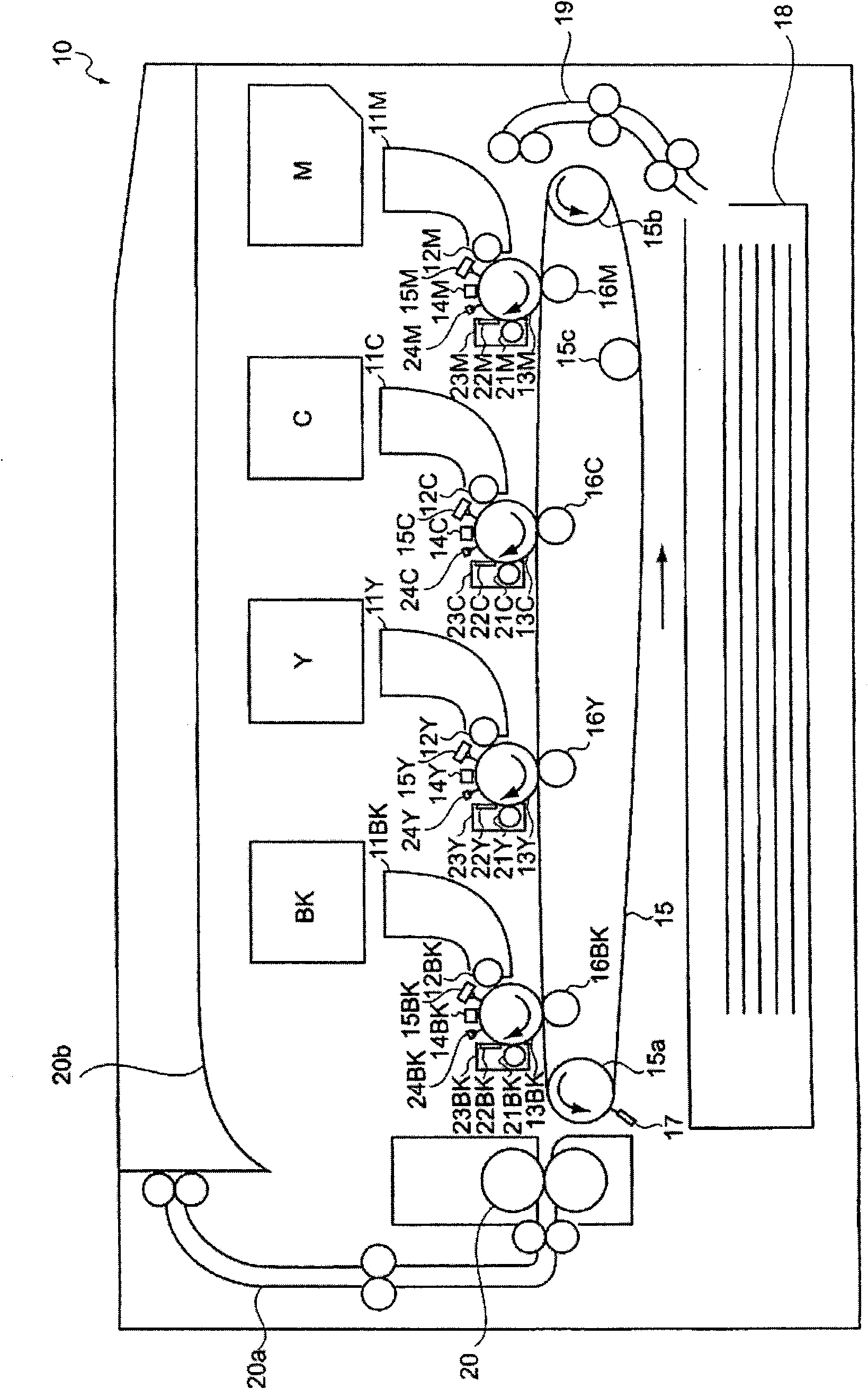
[0157] First, make figure 2 The amorphous silicon photoreceptors 13M to 13BK of the shown full-color image forming apparatus 10 are rotated clockwise as indicated by the arrows in the figure at a predetermined processing speed (peripheral speed), and then charged by the charging devices 14M to 14BK. Its surface carries a defined potential.
[0158] Next, the surfaces of the amorphous silicon photoreceptors 13M to 13BK are exposed through mirrors or the like while performing light modulation according to the image information by the exposure devices 15M to 15BK. By this exposure, electrostatic latent images of respect...
Embodiment 1
[0168] 1. Fabrication of Amorphous Silicon Photoreceptor
[0169] Amorphous silicon photoreceptors were produced under the conditions shown in Table 1 below using RF power of 13.56 MHz in a glow discharge decomposition apparatus.
[0170] Table 1
[0171]
[0172] The * marks in Table 1 indicate relative to SiH 4 gas flow ratio.
[0173] 2. Measurement of solid photoelectric potential
[0174] The amorphous silicon photoreceptor prepared as described above was mounted on figure 2 In the illustrated full-color image forming apparatus 10, the photopotential of a solid was measured.
[0175] That is, the developing device was removed, a potential probe was attached to the developing position, and the surface potential at the developing position was measured when a solid image (solid image) was formed. In addition, the image forming conditions are as follows.
[0176] Surface potential: 300V
[0177] Luminous flux on amorphous silicon photoreceptor: 0.9μJ / cm2
[0178] ...
PUM
 Abstract
Description
Claims
Application Information
 - R&D
- Intellectual Property
- Life Sciences
- Materials
- Tech Scout
- Unparalleled Data Quality
- Higher Quality Content
- 60% Fewer Hallucinations
Browse by: Latest US Patents, China's latest patents, Technical Efficacy Thesaurus, Application Domain, Technology Topic, Popular Technical Reports.
© 2025 PatSnap. All rights reserved.Legal|Privacy policy|Modern Slavery Act Transparency Statement|Sitemap|About US| Contact US: help@patsnap.com