


Quick Research
Generate reliable direction feasibility study reports for your R&D in just a few steps.

Technical Q&A
Discover and master advanced knowledge NOW. Basics, ideas, possibilities, all at once.

Find Solutions
As an expert in R&D theories, this can generate solutions to your technical problems instantly.

Evaluate Feasibility
Analyze your overall solution with one click, know your potential R&D risks in advance.

Monitor Landscape
Get weekly tech updates, stay abreast of the latest tech innovations and key insights.
Semiconductor wafer surface protection tape and semiconductor wafer processing method
A processing method, semiconductor technology, applied in semiconductor/solid-state device manufacturing, metal processing equipment, film/sheet adhesive, etc., can solve problems such as residual glue, achieve easy peeling, suppress residual glue, prevent dust or The effect of penetration of grinding water
- Summary
- Abstract
- Description
- Claims
- Application Information
AI Technical Summary
Problems solved by technology
Method used
Image

Examples
Embodiment
[0097] Hereinafter, the present invention will be described in more detail based on examples, but the present invention is not limited to these examples.
[0098] >
preparation example 1
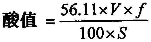
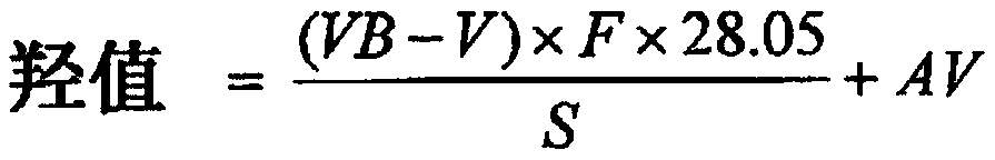
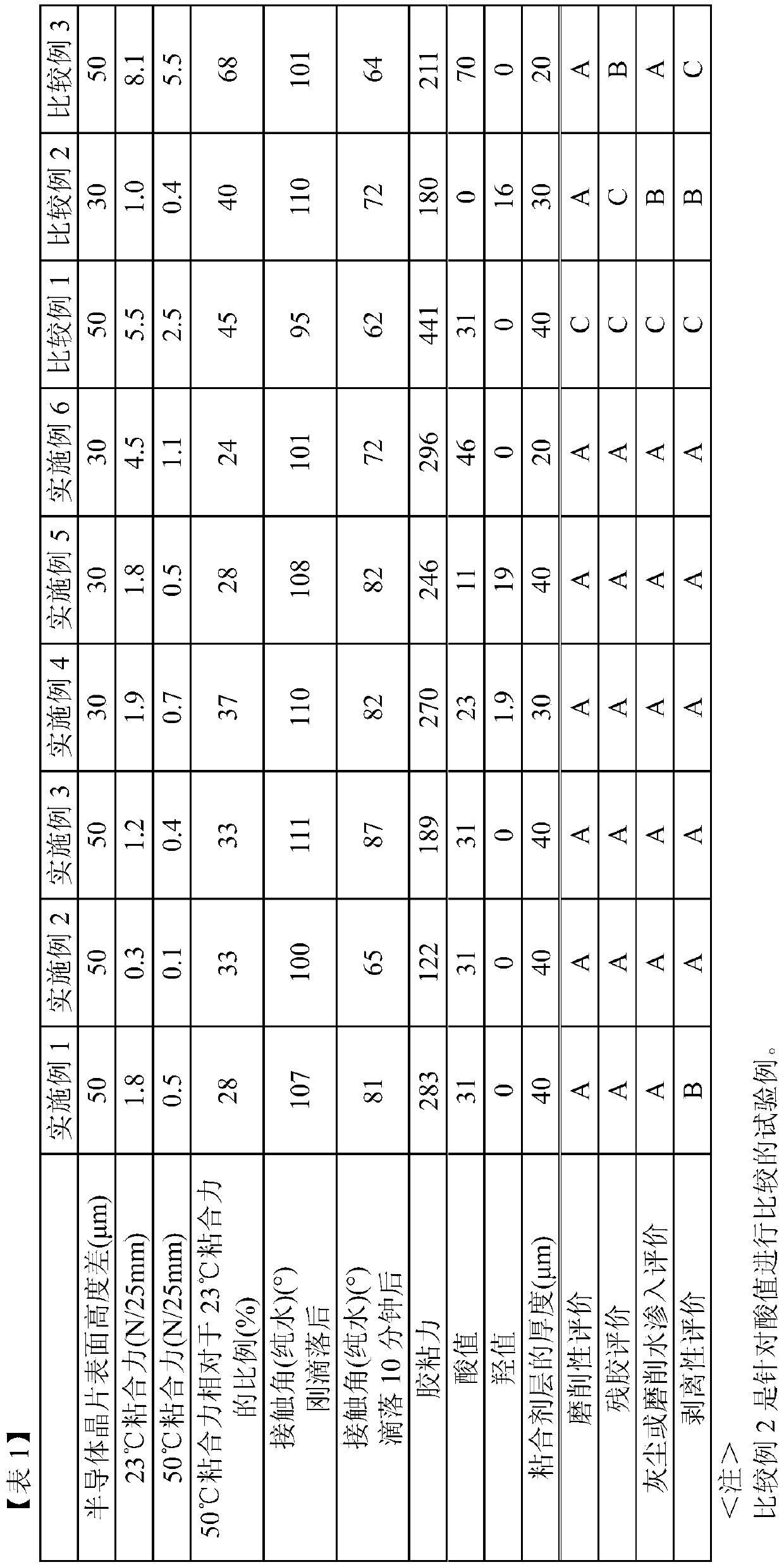
[0100] 90 parts by mass of 2-ethylhexyl acrylate, 5 parts by mass of methyl methacrylate, and 5 parts by mass of methacrylic acid were reacted in ethyl acetate at 55° C. for 10 hours to polymerize. 100 parts by mass of a (meth)acrylic polymer having a weight average molecular weight of 500,000, 0.5 parts by mass of an isocyanate curing agent (manufactured by Nippon Polyurethane, trade name "Coronate L"), 0.5 parts by mass of an epoxy curing agent (manufactured by Mitsubishi Gas Chemical Co., Ltd. , trade name "Tetrad C") 0.6 parts by mass to obtain an adhesive composition. The hydroxyl value is 0mgKOH, and the acid value is 31mgKOH.
[0101] In addition, the measurement conditions by the GPC method of a weight average molecular weight are shown below.
[0102] [Measurement conditions by GPC method]
[0103] Equipment used: High performance liquid chromatography LC-20AD [manufactured by Shimadzu Corporation, trade name]
[0104] Column: Shodex Column GPC KF-805 [manufactured...
preparation example 2
[0110] Except having changed the compounding quantity of an epoxy curing agent into 2.2 mass parts, it carried out similarly to the preparation example 1, and obtained the adhesive composition.
PUM
| Property | Measurement | Unit |
|---|---|---|
| acid value | aaaaa | aaaaa |
| hydroxyl value | aaaaa | aaaaa |
| acid value | aaaaa | aaaaa |
Abstract
Description
Claims
Application Information
 - R&D Engineer
- R&D Manager
- IP Professional
- Industry Leading Data Capabilities
- Powerful AI technology
- Patent DNA Extraction
Browse by: Latest US Patents, China's latest patents, Technical Efficacy Thesaurus, Application Domain, Technology Topic, Popular Technical Reports.
© 2024 PatSnap. All rights reserved.Legal|Privacy policy|Modern Slavery Act Transparency Statement|Sitemap|About US| Contact US: help@patsnap.com