Eureka AIR delivers breakthrough ideas for toughest innovation challenges, trusted by R&D personnel around the world.

Preparation method of nanoscale laser array

A laser array, nano-scale technology, used in lasers, laser devices, laser parts, etc., to achieve the effects of strong controllability, good thermal stability, high light absorption and emission efficiency

Inactive Publication Date: 2017-08-29
黄山博蓝特半导体科技有限公司
View PDF6 Cites 14 Cited by
  • Summary
  • Abstract
  • Description
  • Claims
  • Application Information

AI Technical Summary

Problems solved by technology

[0004] The purpose of the present invention is to provide a method for preparing a nanoscale laser array to solve the problem that the nanoscale laser light source obtained by the prior art method cannot be integrated with large-scale high-density photonics

Method used


Image

  • Preparation method of nanoscale laser array
  • Preparation method of nanoscale laser array
  • Preparation method of nanoscale laser array

Examples


Embodiment 1

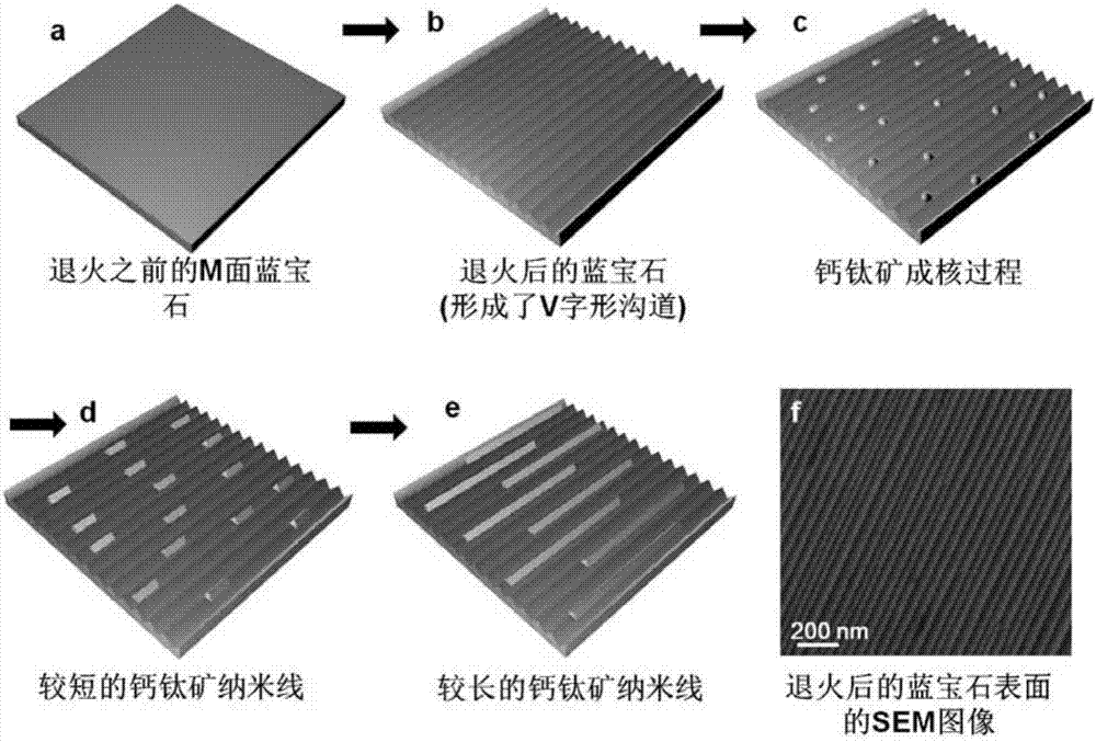
[0039] Example 1, such as Figures 1 to 7 As shown, the preparation of in-plane aligned CsPbBr 3 nanoscale laser array method, the M-Plane sapphire (as attached figure 2 Shown in a) Annealed at 1400°C for 10 hours, then ultrasonically cleaned with acetone, isopropanol, and deionized water for 10 minutes, and finally dried in a nitrogen atmosphere to form a "V"-shaped channel on the surface. as attached figure 2 (b) shown.

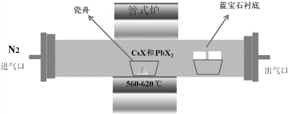
[0040] CsBr and PbBr 2 The powder is mixed according to 1:1 and placed in the No. 1 porcelain boat, and then the porcelain boat is placed in the middle temperature zone of the tube furnace, and the annealed M-face sapphire is placed in the No. 2 porcelain boat and placed downstream low temperature zone. as attached figure 1 As shown, vacuumize and feed high-purity nitrogen to exhaust the oxygen in the system on the one hand, and on the other hand as a carrier gas to raise the temperature of the tube furnace to 620°C, keep the pressure in the tube fu...

Embodiment 2

[0043] A preparation of CsPbI aligned in-plane 3 methods for nanoscale laser arrays, such as Figures 1 to 7 As shown, the M-Plane Sapphire (as attached figure 2 Shown in a) Annealed at 1400°C for 10 hours, then ultrasonically cleaned with acetone, isopropanol, and deionized water for 10 minutes, and finally dried in a nitrogen atmosphere to form a "V"-shaped channel on the surface. as attached figure 2 (b) shown.

[0044] CsI ​​and PbI 2 The powder is mixed according to 2:1 and placed in the No. 1 porcelain boat, and then the porcelain boat is placed in the middle temperature zone of the tube furnace, and the annealed M-surface sapphire is placed in the No. 2 porcelain boat and placed downstream low temperature zone. as attached figure 1 As shown, vacuumize and feed high-purity nitrogen to exhaust the oxygen in the system on the one hand, and on the other hand as a carrier gas to raise the temperature of the tube furnace to 560 ° C, keep the pressure in the tube furna...


PUM

PropertyMeasurementUnit
lengthaaaaaaaaaa
lengthaaaaaaaaaa
diameteraaaaaaaaaa

Abstract

The invention relates to a preparation method of a nanoscale laser array, in particular to a preparation method of a nano laser array using perovskite nanowires in directional alignment as a gain medium and a resonant cavity. The one-dimensional nanoscale perovskite nanowires in directional alignment are used as the gain medium and the resonant cavity, the perovskite nanowires in directional alignment in a plane are successfully prepared, the nanoscale laser array is realized, and the problem of a nanoscale light source in a high-density photon integration system is effectively solved. The chemical formula of the perovskite nanowires in directional alignment is CsPbX3, the diameter is 200 to 800 nm, and the length is 10 to 80 microns. In a synthetic method, CsX powder and PbX2 powder are taken as raw materials, annealed M-Plane sapphire is taken as a substrate, and the nanoscale laser array is prepared by adopting a chemical vapor deposition method. The preparation method also has extremely important significance for realizing the high-density photon integration system.

Description

technical field [0001] The invention relates to a preparation method of a nanoscale laser, in particular to a preparation method of an in-plane nanoscale laser array. Background technique [0002] The perovskite CsPbX3 (X=Cl, Br, I,) nanostructure has been widely used and studied in the fields of light-emitting diodes, lasers and photodetectors due to its excellent photoelectric properties. Most of the existing solution methods are used to obtain CsPbX3 quantum dots, nanosheets, and nanowires. However, the perovskite nanowires obtained by this method are disorderly and irregular in order and have poor crystallinity. The resulting nanoscale lasers have unstable performance. [0003] The traditional chemical vapor deposition method is usually used to synthesize high-quality nanostructure materials, which provides a new idea for the synthesis of high-quality perovskite nanostructures. Recently, researchers have realized high-quality perovskite nanostructures, such as single-cr...

Claims


Application Information

Patent Timeline
Patent Type & Authority Applications(China)
IPC IPC(8): H01S3/16H01S3/23C30B29/12C30B29/60C30B25/18
CPCH01S3/163C30B25/18C30B29/12C30B29/60H01S3/169H01S3/23
Inventor 刘建哲褚君尉祝小林徐良
Owner 黄山博蓝特半导体科技有限公司
Why Eureka
Eureka Blog
Learn More