Heat treatment process method and manufacturing process method for thin-film resistor

A technology of thin film resistors and process methods, which is used in resistor manufacturing, resistors, and coating resistor materials, etc., can solve the problem of poor resistance change rate, large resistance deviation, product resistance to over-stress and over-electricity exposed to high temperature The problem of poor fatigue performance, etc., achieves the effect of good resistance accuracy consistency, improved overcurrent resistance performance, and high pass rate

Active Publication Date: 2017-08-25
CHINA ZHENHUA GRP YUNKE ELECTRONICS
View PDF5 Cites 0 Cited by
  • Summary
  • Abstract
  • Description
  • Claims
  • Application Information

AI Technical Summary

Problems solved by technology

However, there are still at least the following deficiencies: the first point: after laser trimming, the resistance value dispersion is large, which affects the resistance value pass rate of the product; the second point: the product is unstable due to the instability of the film layer , will cause a large resistance shift, a poor resistance change rate exposed to high temperature, and poor performance in high temperature environments; the third point: when the power-on transient overload is performed, due to the large stress of the film layer, plus The stress caused by laser trimming will cause some products to have poor resistance to over-electrical stress and over-electrical fatigue

Method used


Image

  • Heat treatment process method and manufacturing process method for thin-film resistor
  • Heat treatment process method and manufacturing process method for thin-film resistor
  • Heat treatment process method and manufacturing process method for thin-film resistor

Examples


Embodiment 1

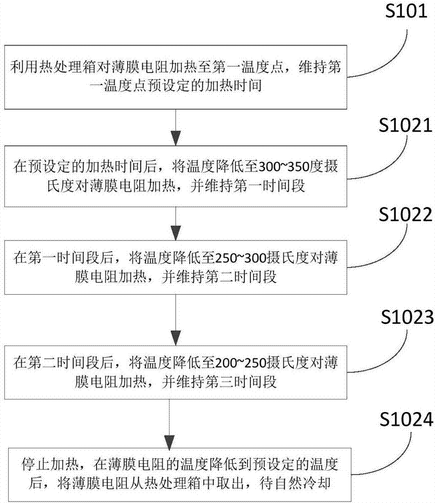
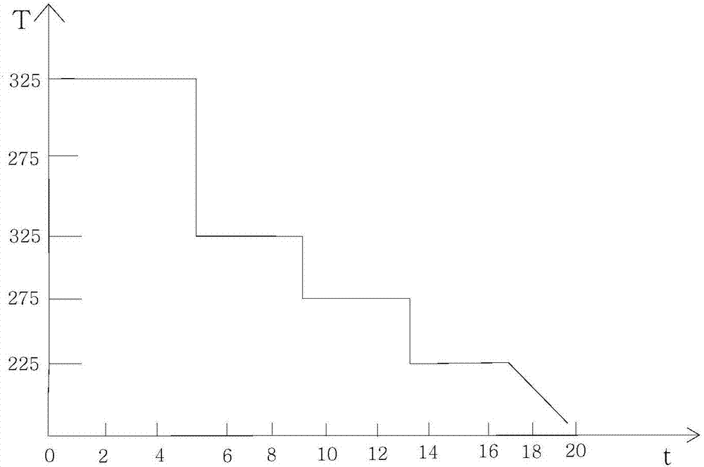
[0055] see figure 1 , an embodiment of the present invention provides a thin film resistance heat treatment process, the thin film resistance heat treatment process comprising:

[0056] Step S101: using a heat treatment box to heat the thin film resistance to a first temperature point, and maintaining the first temperature point for a preset heating time.

[0057] For example, use a heat treatment box to heat the thin film resistance to 390-450 degrees Celsius, and maintain the temperature at 390-450 degrees Celsius for 2h-7h. Of course, the first temperature point can be 390 degrees Celsius or 425 degrees Celsius or 450 degrees Celsius, and there is no limit here, as long as it is between 390 and 450 degrees Celsius, the heating time can be 2h, 4.5h or 7h, and there is no limit here , as long as it is within the range of 2h ~ 7h.

[0058] Step S102: After a preset heating time, at least one second temperature point is used to cool down the thin film resistor for a preset co...

Embodiment 2

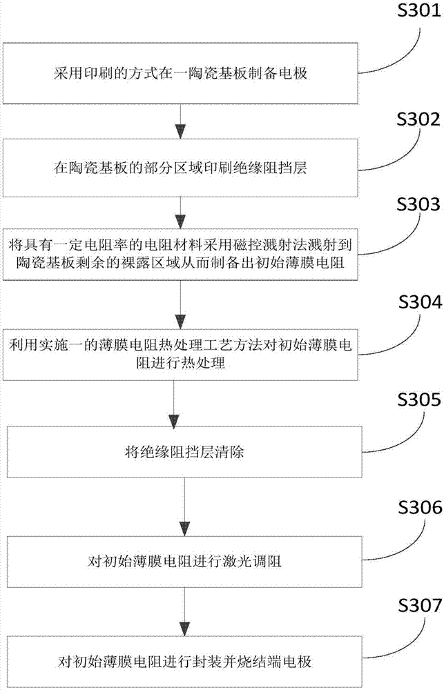
[0071] see image 3 , the embodiment of the present invention also provides a thin film resistor manufacturing process method, the thin film resistor manufacturing process method includes:

[0072] Step S301: Prepare electrodes on a ceramic substrate by printing.

[0073] Step S302: printing an insulating barrier layer on a part of the ceramic substrate.

[0074] Step S303: Sputtering a resistive material with a certain resistivity onto the remaining exposed area of ​​the ceramic substrate by magnetron sputtering to prepare an initial thin film resistor.

[0075] Step S304: performing heat treatment on the initial thin film resistor by using the above thin film resistor heat treatment process.

[0076] Step S305: removing the insulating barrier layer.

[0077] For example, the insulating barrier layer is washed off with clean water.

[0078] Step S306: performing laser trimming on the initial thin film resistance.

[0079] Step S307: Encapsulating the initial thin film re...


PUM


Abstract

The invention provides a heat treatment process method and manufacturing process method for a thin-film resistor and relates to the field of electronic components. The heat treatment process method and manufacturing process method for the thin-film resistor comprise the following steps: heating a thin-film resistor to a first temperature point by utilizing a heat treatment box, and maintaining heating time preset at the first temperature point; cooling the thin-film resistor for preset cooling time by adopting at least one second temperature point after the preset heating time, wherein the preset cooling time comprises cooling time periods of which the number is the same as the quantity of the temperature points, and the at least one second temperature point is sequentially decreased progressively according to a sequence of the cooling time periods. Therefore, the finally produced thin-film resistor has high resistance precision consistency and high yield. Moreover, the over-current resistance, fatigue resistance and high-temperature exposure performance of the thin-film resistor are improved.

Description

technical field [0001] The invention relates to the field of electronic components, in particular to a thin film resistance heat treatment process method and manufacturing process method. Background technique [0002] Thin film resistors are made by evaporating a certain resistivity material on the surface of an insulating material by a similar evaporation method. The commonly used insulating material for thin film resistors is a ceramic substrate. Thin-film resistors are commonly used in various instruments and meters, medical equipment, power supplies, power equipment, and electronic digital products. Unlike thick-film resistors, thick-film resistors generally use screen printing technology, and thin-film resistors use vacuum evaporation and magnetron sputtering. Injection and other process methods. Thick film resistors generally have poor precision, 10%, 5%, and 1% are common precisions, while thin film resistors can achieve 0.01% one-thousandth precision, 0.1% one-thous...

Claims


Application Information

Patent Timeline
Patent Type & Authority Applications(China)
IPC IPC(8): H01C17/00H01C17/12H01C17/242H01C17/28H01C17/30
CPCH01C17/00H01C17/12H01C17/242H01C17/28H01C17/30
Inventor 芮家群罗彦军韩玉成程德雁希毅侯本昌
Owner CHINA ZHENHUA GRP YUNKE ELECTRONICS
Why Eureka
Try Eureka