A kind of preparation method of silicon carbide surface oxide film
A technology of surface oxidation and silicon carbide, applied in semiconductor/solid-state device manufacturing, electrical components, circuits, etc., can solve the problems of SiCMOSFET device performance degradation, complex oxidation mechanism, etc., to reduce the interface state density, the process is simple, and the quality is improved. Effect
- Summary
- Abstract
- Description
- Claims
- Application Information
AI Technical Summary
Problems solved by technology
Method used
Image

Examples
Embodiment 1
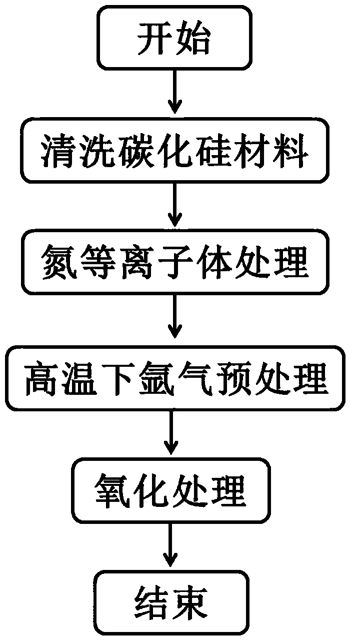
[0031] A method for preparing an oxide film on a silicon carbide surface, the method comprising the steps of:
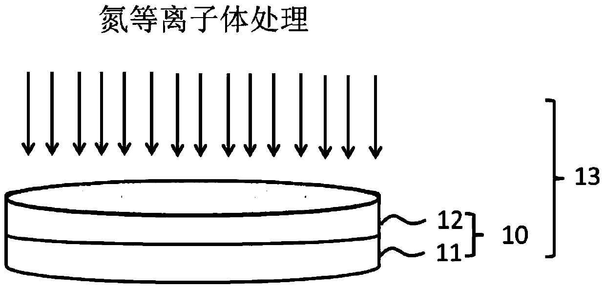
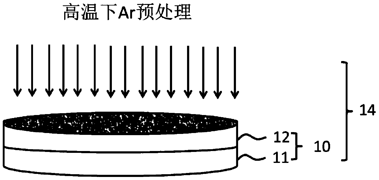
[0032] 1) Clean the silicon carbide material 10, the silicon carbide material 10 includes a substrate 11 and an epitaxial film 12, the substrate 11 in the silicon carbide material 10 is n-type 4H-SiC, the thickness is about 380 μm, n-type doped impurities Nitrogen (N), the doping concentration is about 5×10 18 cm -3 ; The epitaxial film 12 in the silicon carbide material 10 is n-type 4H-SiC with a thickness of about 12 μm, and the n-type doped impurity is nitrogen (N), and the doping concentration is about 8×10 15 cm -3 ;
[0033] The silicon carbide material 10 is cleaned by the RCA standard cleaning method, and the specific cleaning steps are as follows:
[0034] (1) Prepare hydrofluoric acid solution (HF:H 2 O=1:10);
[0035] (2) The sample holder is cleaned and dried for use;
[0036] (3) Take the silicon carbide sample 10 and put it on the support, and pu...
Embodiment 2
[0049] A method for preparing an oxide film on a silicon carbide surface, the method comprising the steps of:
[0050]1) Clean the silicon carbide material 10, the silicon carbide material 10 includes a substrate 11 and an epitaxial film 12, the substrate 11 in the silicon carbide material 10 is n-type 4H-SiC, the thickness is about 300 μm, n-type doped impurities Nitrogen (N), the doping concentration is about 5×10 20 cm -3 ; The epitaxial film 12 in the silicon carbide material 10 is n-type 4H-SiC with a thickness of about 15 μm, and the n-type doped impurity is nitrogen (N), and the doping concentration is about 8×10 18 cm -3 ;
[0051] The silicon carbide material 10 is cleaned by the RCA standard cleaning method, and the specific cleaning steps are as follows:
[0052] (1) Prepare hydrofluoric acid solution (HF:H 2 O=1:10);
[0053] (2) The sample holder is cleaned and dried for use;
[0054] (3) Take the silicon carbide sample 10 and put it on the support, and put...
Embodiment 3
[0067] A method for preparing an oxide film on a silicon carbide surface, the method comprising the steps of:
[0068] 1) Cleaning the silicon carbide material 10, the silicon carbide material 10 includes a substrate 11 and an epitaxial film 12, the substrate 11 in the silicon carbide material 10 is n-type 6H-SiC, the thickness is about 450 μm, n-type doped impurities Nitrogen (N), the doping concentration is about 5×10 18 cm -3 ; The epitaxial thin film 12 in the silicon carbide material 10 is n-type 6H-SiC, the thickness is about 15 μm, the n-type doping impurity is nitrogen (N), and the doping concentration is about 8×10 15 cm -3 ;
[0069] The silicon carbide material 10 is cleaned by the RCA standard cleaning method, and the specific cleaning steps are as follows:
[0070] (1) Prepare hydrofluoric acid solution (HF:H 2 O=1:10);
[0071] (2) The sample holder is cleaned and dried for use;
[0072] (3) Take the silicon carbide sample 10 and put it on the support, and...
PUM
| Property | Measurement | Unit |
|---|---|---|
| thickness | aaaaa | aaaaa |
| thickness | aaaaa | aaaaa |
| thickness | aaaaa | aaaaa |
Abstract
Description
Claims
Application Information
 - Generate Ideas
- Intellectual Property
- Life Sciences
- Materials
- Tech Scout
- Unparalleled Data Quality
- Higher Quality Content
- 60% Fewer Hallucinations
Browse by: Latest US Patents, China's latest patents, Technical Efficacy Thesaurus, Application Domain, Technology Topic, Popular Technical Reports.
© 2025 PatSnap. All rights reserved.Legal|Privacy policy|Modern Slavery Act Transparency Statement|Sitemap|About US| Contact US: help@patsnap.com