High-conductivity graphene/copper-based layered composite material and preparation method thereof
A composite material and graphene technology, applied in the direction of metal layered products, chemical instruments and methods, metal material coating technology, etc., can solve the problems that are not conducive to graphene's high electron mobility, increased carrier scattering, and low conductivity And other problems, to achieve the effect of high utilization efficiency, overcome the reduction of resistance, and easy production
- Summary
- Abstract
- Description
- Claims
- Application Information
AI Technical Summary
Problems solved by technology
Method used
Image
Examples
Embodiment 1
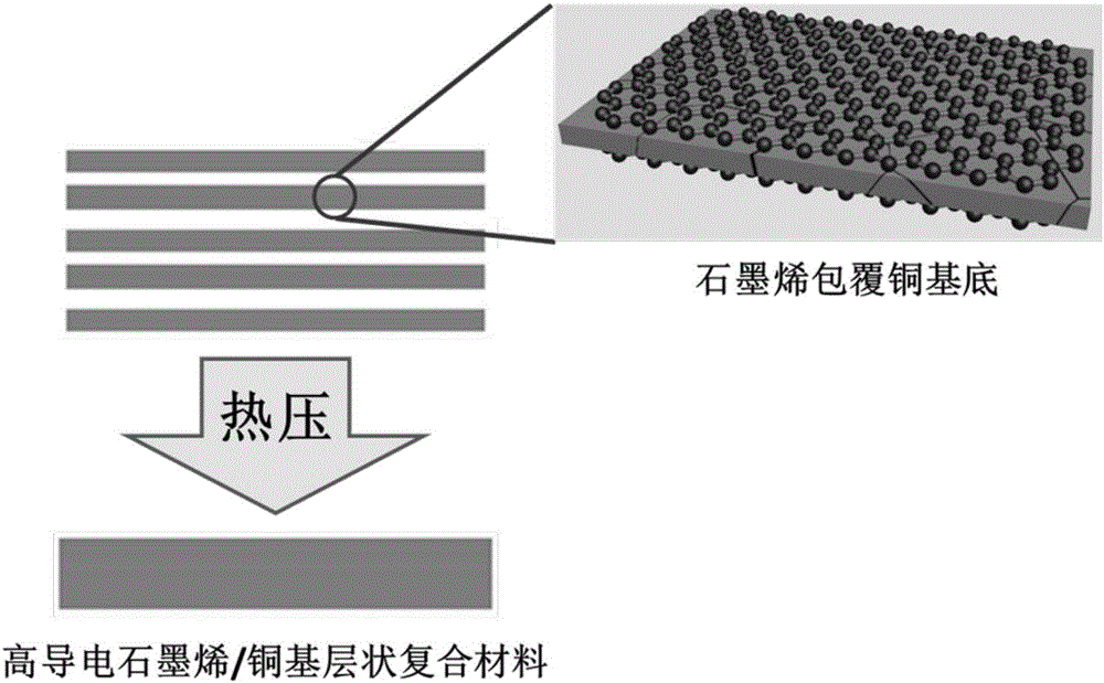
[0034] First, graphene with a thickness of a single layer and a coverage of ≥95% is grown on the surface of a 500 μm thick copper substrate by chemical vapor deposition, and the carbon source is methane gas to obtain a sandwich-shaped graphene-coated copper substrate. The particle size is ≥300 μm; then two graphene-coated copper substrates are vacuum hot-pressed and sintered to obtain a highly conductive graphene / copper-based laminated composite material. The conductivity of the obtained layered composite is (66.2×10 6 S / m, 114%IACS), higher than pure silver, meeting the requirements for use.
Embodiment 2
[0036] First, graphene with a thickness of a single layer and a coverage of ≥95% is grown on the surface of a 100 μm thick copper substrate by chemical vapor deposition, and the carbon source is acetylene gas to obtain a sandwich-shaped graphene-coated copper substrate with in-plane grains. The particle size is ≥300 μm; and then 5 graphene-coated copper substrates are hot-pressed and sintered under the protection of an argon atmosphere to obtain a highly conductive graphene / copper-based laminated composite material. The conductivity of the obtained layered composite is (67.2×10 6 S / m, 116%IACS), higher than pure silver, meeting the requirements for use.
Embodiment 3
[0038] First, graphene with a thickness of a single layer and a coverage ≥ 95% is grown on the surface of a 40 μm thick copper substrate by chemical vapor deposition, and the carbon source is methane gas to obtain a sandwich-shaped graphene-coated copper substrate with in-plane grains The particle size is ≥300 μm; then 10 graphene-coated substrates are subjected to spark plasma sintering to obtain a highly conductive graphene / copper-based composite material. The conductivity of the obtained layered composite is (66.9×10 6 S / m, 115%IACS), higher than pure silver, meeting the requirements for use.
PUM
| Property | Measurement | Unit |
|---|---|---|
| Grain size | aaaaa | aaaaa |
| Conductivity | aaaaa | aaaaa |
| Conductivity | aaaaa | aaaaa |
Abstract
Description
Claims
Application Information
 - R&D
- Intellectual Property
- Life Sciences
- Materials
- Tech Scout
- Unparalleled Data Quality
- Higher Quality Content
- 60% Fewer Hallucinations
Browse by: Latest US Patents, China's latest patents, Technical Efficacy Thesaurus, Application Domain, Technology Topic, Popular Technical Reports.
© 2025 PatSnap. All rights reserved.Legal|Privacy policy|Modern Slavery Act Transparency Statement|Sitemap|About US| Contact US: help@patsnap.com


