Nanoporous copper/cu(oh)2 nanowire array sensor electrode material and preparation method thereof
A nanoporous copper and nanowire array technology, applied in the field of micro-sensing, can solve problems such as easy agglomeration and poor electrical conductivity, and achieve the effects of increasing the contact area, overcoming poor electrical conductivity, and simple preparation methods
- Summary
- Abstract
- Description
- Claims
- Application Information
AI Technical Summary
Problems solved by technology
Method used
Image
Examples
Embodiment 1
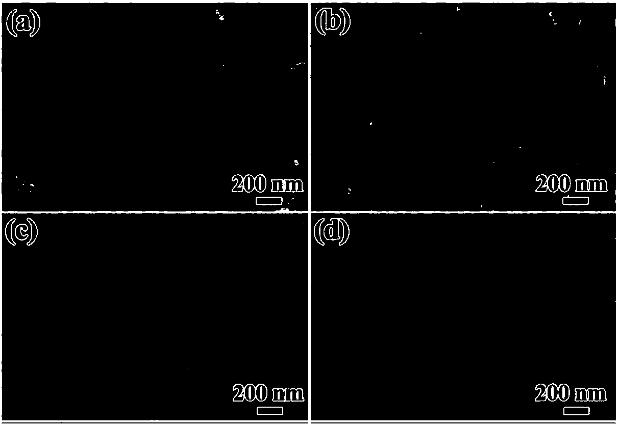
[0034] Take Cu x Zr 95-x Al 5 (x=30, x=40, x=50 and x=60) as the nominal composition of the precursor alloy, the pure elements required for the precursor alloy (Cu 99.99 wt%, Zr 99.99 wt%, Al 99.99 wt%), Convert the atomic percentage of the alloy into mass (10g) and weigh it, and then use the method of high-purity argon atmosphere vacuum arc melting to obtain Cu x Zr 95-x Al 5 (x=30, x=40, x=50 and x=60) master alloy button ingots, smelting 3~4 times to ensure uniform composition of master alloy ingots. The master alloy ingots are re-melted by induction heating in a quartz tube, and are continuously and rapidly sprayed onto a water-cooled rotating copper roller under the action of high-purity argon at a pressure of about 0.2 MPa to form Cu x Zr 95-x Al 5 (x=30, x=40, x=50 and x=60) fast-quenched amorphous alloy thin strips, the thickness of the amorphous thin strip is about 20-25 μm, and the width is 5-6 mm.
[0035] Take Cu x Zr 95-x Al 5 (x=30, x=40, x=50 and x=60...
Embodiment 2
[0038] Take Cu 60 Z 35 Al 5 As the nominal composition of the precursor alloy, the pure elements required for the precursor alloy (Cu 99.99wt%, Zr 99.99wt%, Al 99.99wt%) were weighed according to the atomic percentage of the alloy into mass (10g), and then the high The method of pure argon atmosphere vacuum arc smelting, smelting to obtain Cu 40 Z 55 Al 5 Master alloy button ingots are smelted 3 to 4 times to ensure uniform composition of master alloy ingots. The master alloy ingot is re-melted by induction heating in a quartz tube, and is continuously and rapidly sprayed onto a water-cooled rotating copper roller under the action of high-purity argon at a pressure of about 0.2 MPa to form Cu 60 Z 35 Al 5 Rapidly Quenched Amorphous Alloy Ribbon.
[0039] Take Cu 60 Z 35 Al 5 Amorphous alloy thin strips were used as precursors, and 0.005mol / L HF aqueous solution was used as corrosion solution for chemical dealloying. Before treatment, amorphous alloy thin strips were...
Embodiment 3
[0041] Take Cu 60 Z 35 Al 5 As the nominal composition of the precursor alloy, the pure elements required for the precursor alloy (Cu 99.99wt%, Zr 99.99wt%, Al 99.99wt%) were weighed according to the atomic percentage of the alloy into mass (10g), and then the high The method of pure argon atmosphere vacuum arc smelting, smelting to obtain Cu 60 Z 35 Al 5 Master alloy button ingots are smelted 3 to 4 times to ensure uniform composition of master alloy ingots. The master alloy ingot is re-melted by induction heating in a quartz tube, and is continuously and rapidly sprayed onto a water-cooled rotating copper roller under the action of high-purity argon at a pressure of about 0.2 MPa to form Cu 60 Z 35 Al 5 Rapidly Quenched Amorphous Alloy Ribbon.
[0042] Take Cu 60 Z 35 Al 5 Amorphous alloy thin strips were used as precursors, and 0.005mol / L HF aqueous solution was used as corrosion solution for chemical dealloying. Before treatment, amorphous alloy thin strips were...
PUM
| Property | Measurement | Unit |
|---|---|---|
| Sensitivity | aaaaa | aaaaa |
| pore size | aaaaa | aaaaa |
| thickness | aaaaa | aaaaa |
Abstract
Description
Claims
Application Information
 - Generate Ideas
- Intellectual Property
- Life Sciences
- Materials
- Tech Scout
- Unparalleled Data Quality
- Higher Quality Content
- 60% Fewer Hallucinations
Browse by: Latest US Patents, China's latest patents, Technical Efficacy Thesaurus, Application Domain, Technology Topic, Popular Technical Reports.
© 2025 PatSnap. All rights reserved.Legal|Privacy policy|Modern Slavery Act Transparency Statement|Sitemap|About US| Contact US: help@patsnap.com


