Crystalline silicon solar cell and preparation method thereof
A technology for solar cells and crystalline silicon, applied in circuits, electrical components, semiconductor devices, etc., can solve the problems of weakening the passivation layer on the photoelectric performance of the battery, increasing the series resistance of the battery, and expensive equipment, and improving the photoelectric conversion efficiency. , the short-circuit current Isc increase, the effect of fast deposition
- Summary
- Abstract
- Description
- Claims
- Application Information
AI Technical Summary
Problems solved by technology
Method used
Image
Examples
preparation example Construction
[0033] The present invention also provides a method for preparing the above-mentioned crystalline silicon solar cell, which specifically includes the following steps:
[0034] S1. Provide a silicon substrate with a diffusion layer on the light-facing surface, and deposit boron carbide or cubic boron nitride on the backlight surface of the silicon substrate to form a passivation layer;
[0035] S2. Prepare an aluminum back field on the passivation layer, and the aluminum back field penetrates the passivation layer and is in contact with the silicon substrate;
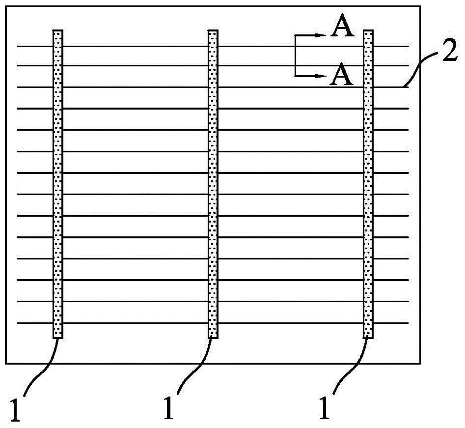
[0036] S3. Prepare the electrode grid lines on the backlight surface on the aluminum back field, and prepare the electrode grid lines on the light-facing surface in contact with the diffusion layer on the light-facing surface of the silicon substrate.
[0037] The method provided by the invention is prepared on the basis of a silicon substrate with a diffusion layer on the light-facing surface. Wherein, the silicon subs...
Embodiment 1
[0062] This embodiment is used to illustrate the crystalline silicon solar cell and its preparation method disclosed in the present invention.
[0063] 1. Preparation of silicon wafers before plating passivation layer
[0064] The specification of the polycrystalline silicon wafer used is: 156mm×156mm, and the thickness is 200μm. After the silicon wafer is textured, diffused and etched, the back of the silicon wafer is polished to obtain a silicon substrate with a diffusion layer on the surface.
[0065] 2. Preparation of silicon nitride anti-reflection coating on the smooth surface
[0066] Silicon nitride anti-reflection coating is coated by ordinary low-frequency induced plasma chemical vapor deposition (LP-PECVD). The nitrogen source is ammonia gas, the silicon source is silane, the working frequency is 380kHz, and the working temperature of the silicon substrate is 440°C. The flow ratio of silane is 12:1, the radio frequency power is 2900W, and the deposition time is 9.5...
Embodiment 2
[0076] This embodiment is used to illustrate the crystalline silicon solar cell and its preparation method disclosed in the present invention.
[0077] Change the deposition time of the boron carbide passivation layer in step 3 in embodiment 1 to 25min, so that the thickness of the passivation layer becomes 190-200nm, and the rest are the same as in embodiment 1.
[0078] The obtained crystalline silicon solar cell is denoted as S2.
PUM
| Property | Measurement | Unit |
|---|---|---|
| thickness | aaaaa | aaaaa |
| width | aaaaa | aaaaa |
| thickness | aaaaa | aaaaa |
Abstract
Description
Claims
Application Information
 - R&D Engineer
- R&D Manager
- IP Professional
- Industry Leading Data Capabilities
- Powerful AI technology
- Patent DNA Extraction
Browse by: Latest US Patents, China's latest patents, Technical Efficacy Thesaurus, Application Domain, Technology Topic, Popular Technical Reports.
© 2024 PatSnap. All rights reserved.Legal|Privacy policy|Modern Slavery Act Transparency Statement|Sitemap|About US| Contact US: help@patsnap.com


