


Quick Research
Generate reliable direction feasibility study reports for your R&D in just a few steps.

Technical Q&A
Discover and master advanced knowledge NOW. Basics, ideas, possibilities, all at once.

Find Solutions
As an expert in R&D theories, this can generate solutions to your technical problems instantly.

Evaluate Feasibility
Analyze your overall solution with one click, know your potential R&D risks in advance.

Monitor Landscape
Get weekly tech updates, stay abreast of the latest tech innovations and key insights.
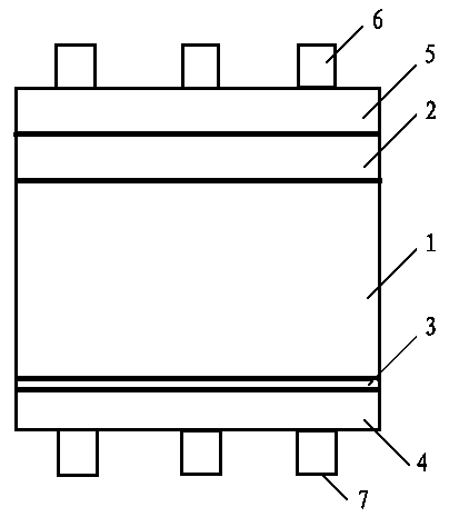
Crystalline silicon solar cell subjected to back polishing and preparation technology thereof
A technology for solar cells and back polishing, which is applied in the field of solar cells, can solve problems such as poor metal contact, and achieve the effects of low manufacturing cost, enhanced reflection, and simple preparation methods
- Summary
- Abstract
- Description
- Claims
- Application Information
AI Technical Summary
Problems solved by technology
Method used
Image

Examples
preparation example Construction
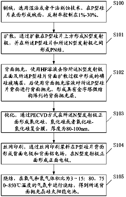
[0056] Correspondingly, the present invention also provides a method for preparing a back-polished crystalline silicon solar cell as claimed in claim 1, such as image 3 shown, including the following steps:
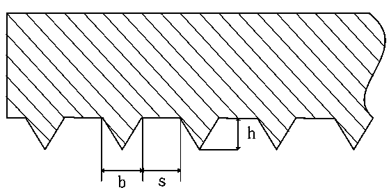
[0057] S100 texturing adopts wet or dry etching technology to form a textured surface on the surface of the P-type silicon wafer, and the reflectivity is controlled at 1%-30%.
[0058] S101 Diffusion, forming an N-type emitter above the P-type silicon slice through diffusion, and forming a PN junction between the P-type silicon slice and the N-type emitter.
[0059] Preferably, the sheet resistance needs to be controlled to be 75-100 ohm / □ during diffusion.
[0060] More preferably, the sheet resistance needs to be controlled to be 85-90 ohm / □ during diffusion.
[0061] S102 back polishing, using HF solution to remove the phosphosilicate glass layer formed in the front of the N-type emitter and the back of the P-type silicon wafer during the diffusion process, and then...
Embodiment 1
[0085] (1) For texturing, use wet or dry etching technology to form a textured surface on the surface of the P-type silicon wafer, and the reflectivity is controlled at 10%;
[0086] (2) Diffusion, through POCl 3 Diffusion forms a PN junction, and the N-type emitter is obtained after controlling the sheet resistance to 75 ohm / □;
[0087] (3) Back polishing, first use HF solution to remove the phosphosilicate glass layer of the P-type silicon wafer, and then polish the back of the P-type silicon wafer with a back polishing solution. The reaction temperature is 80 ° C, and the thickness reduction is 4 μm Then use HF solution to remove the phosphosilicate glass layer on the front of the N-type emitter, after cleaning, dry the surface with hot nitrogen, and finally form a back polishing layer on the back of the P-type silicon wafer.
[0088] (4) Passivation, forming a silicon oxide, silicon nitride or silicon oxide-silicon nitride composite film on the front of the N-type emitter...
Embodiment 2
[0092] (1) For texturing, wet or dry etching technology is used to form a textured surface on the surface of the P-type silicon wafer, and the reflectivity is controlled at 20%;
[0093] (2) Diffusion, through POCl 3 Diffusion forms a PN junction, and the N-type emitter is obtained after controlling the sheet resistance to 80 ohm / □;
[0094] (3) Back polishing, first use HF solution to remove the phosphosilicate glass layer of the P-type silicon wafer, and then polish the back of the P-type silicon wafer with a back polishing solution. The reaction temperature is 82 ° C, and the thickness reduction is 5 μm Then use HF solution to remove the phosphosilicate glass layer on the front of the N-type emitter, after cleaning, dry the surface with hot nitrogen, and finally form a back polishing layer on the back of the P-type silicon wafer.
[0095](4) Passivation, forming a silicon oxide, silicon nitride or silicon oxide-silicon nitride composite film on the front of the N-type emit...
PUM
| Property | Measurement | Unit |
|---|---|---|
| Bottom length | aaaaa | aaaaa |
| Height | aaaaa | aaaaa |
| Thickness | aaaaa | aaaaa |
Abstract
Description
Claims
Application Information
 - R&D Engineer
- R&D Manager
- IP Professional
- Industry Leading Data Capabilities
- Powerful AI technology
- Patent DNA Extraction
Browse by: Latest US Patents, China's latest patents, Technical Efficacy Thesaurus, Application Domain, Technology Topic, Popular Technical Reports.
© 2024 PatSnap. All rights reserved.Legal|Privacy policy|Modern Slavery Act Transparency Statement|Sitemap|About US| Contact US: help@patsnap.com